Description
Who Supplies Wifi PCB Antenna Design?
The Wifi PCB Antenna Design & antenna manufacturing service is provided by C&T RF Antennas Inc. the indoor Wifi PCB Antenna Design and outdoor Omni Wifi Antenna Design service supplier in China.
We not only provide the Wifi PCB Antenna Design but also Flexible Wifi PCB Antenna Design, Not only 2.4 GHz wifi PCB antenna design but also 5.8 GHz wifi PCB antenna design.
The Standard embedded antenna Wi-Fi/BlueTooth PCB antennas can be designed into many PCB antenna types.
How to make a 2.4Ghz Bluetooth/wifi PCB antenna design?
Wifi PCB Antenna Design Operating Frequency:
Bluetooth/wifi operates at 2.4Ghz center frequency is taken as 2.45Ghz
Wifi PCB Antenna Design Length:
At 2.45Ghz 1/4 each free-space wavelength: 30.6mm 1/4 FR4 dielectric wavelength: 14.8mm
Take the middle value of the two 22.7mm where the vertical length of 8mm, the horizontal length of 14.7mm
Analyze the antenna length and resonant frequency to find out the exact length of the antenna working at 2.45Ghz
Analyze the effect of Wifi PCB Antenna Design related parameters change on PCB antenna performance
1. Analyze the effect of PCB board thickness on antenna performance
2. Analyze the effect of ground plane size on antenna performance
3. Analyze the effect of antenna line width on antenna performance
4. Analyze the effect of the total length of an antenna on antenna performance, the effect of vertical length, and horizontal length change on antenna performance
C&T RF Antennas Inc provides wireless antennas with other antenna radio frequencies such as 169MHz, 230MHz, 315MHz, 433MHz, 868MHz, 915MHz, Lora, VHF&UHF, NB-IoT, GSM, Wifi 2.4GHz, 5.8GHz, 2G 3G 4G LTE, GPS, 5G NR, UWB, etc.
We provide the Wifi antenna with many antenna types such as Dipole Antennas, Whip Antennas, Marine Antennas, Router Antennas, MIMO Antennas, PCB Antennas, FPC Antennas, Spring Antennas, etc.
The Wifi PCB Antenna Design and wifi antenna production is supplied by C&T RF Antennas Inc, we also provide the 4G PCB Antenna Design, Lora Antenna Design, NB-IoT Antenna Design, etc.
Contact us for more details on the details of Wifi PCB Antenna Design by Antenna Manufacturing Company C&T RF Antennas Inc.
Wifi PCB Antenna Design Specifications
Wifi PCB Antenna Design Electrical Specifications |
|
| RF Antenna Type | Embedded PCB Antenna |
| Model | CTRF-ANTENNA-PCB-DESIGN |
| Frequency | 2400-2500 MHz; 5150-5800 MHz |
| Gain | Custom |
| VSWR | ≤2.0 |
| Impedance | 50 Ω |
| Polarization | Vertical Polarization |
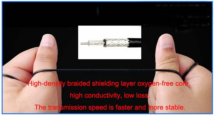
| Cable Type | Custom |
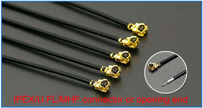
| Connector | U.FL/IPEX |
| Cable Length | Custom |
| Lightning Protection | DC-Ground |
Wifi PCB Antenna Design Mechanical Specifications |
|
| PCB Board Dimension | Custom |
| Weight | Custom |
| Material | PCB |
| Operation Temperature | -40˚C ~ +85˚C |
| Storage Temperature | -40˚C ~ +80˚C |
| Color | Custom |
| Antenna Design | Dipole Array |
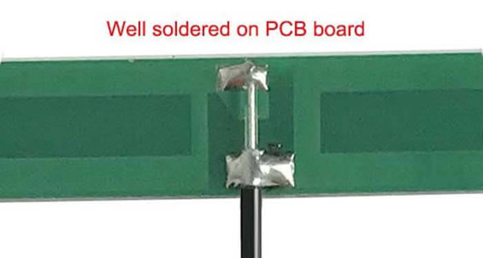
| Mounting | Connector |
| Safety Emission and other | RoHS Compliant |
| Applications | ISM/SCADA/Utilities, IoT/NB-IoT/LoRa, Wi-Fi |
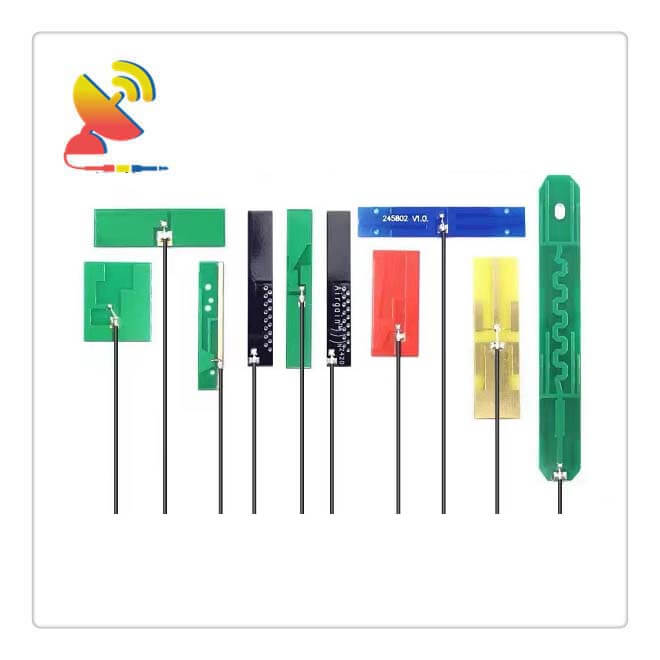
Below are the single-band Wifi PCB Antenna Designed styles:
32×6.5mm(PCB Antenna) Internal 2.4 Ghz Antenna PCB Circuit Board Antenna
47x7mm(PCB Antenna) Internal Bluetooth Antenna 2.4GHz Wifi PCB Antenna
42x12mm(PCB Antenna) 802.11 Antenne Wifi 2.4 GHz Embedded PCB Antenna
25x22mm(PCB Antenna) Omni Dipole Wi-Fi Antenna 2.4 GHz PCB Trace Antenna
33x6mm(PCB Antenna) 2.4 GHz Bluetooth Antenna Internal PCB Antenna Design
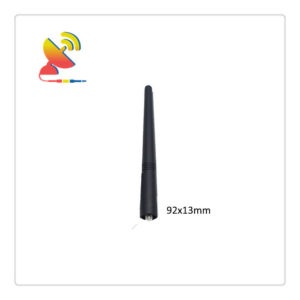
50x15mm(PCB Antenna) Wifi PCB Antenna
48x11mm(PCB Antenna) PCB Wifi Antenna
45x3mm(PCB Antenna) Ipex Wifi Antenna
72x5mm(PCB Antenna) Ipex MHF4 Antenna
Below are the existing dual-band Wifi PCB Antenna Design styles for your choice.
42x12mm(PCB Antenna) PCB Antenna Dual-band Wifi Antenna
48x14mm(PCB Antenna) Embedded PCB Antenna Dual Wifi Antenna
49x8mm(PCB Antenna) PCB Antenna Wifi Dual-band Antenna
25x22mm(PCB Antenna) PCB Wifi Antenna On Board Antenna
40x8mm(PCB Antenna) PCB Trace Antenna Dual Wifi Antenna
25x22mm(PCB Antenna) 2.4 GHz And 5 GHz PCB Antenna
39x7mm(PCB Antenna) Wifi 2.4 GHz 5 GHz PCB Antenna
42x12mm(PCB Antenna) 2.4 GHz 5GHz Wifi PCB Antenna
49x8mm(PCB Antenna)-B 2.4 5GHz Wifi PCB Antenna
52x7mm(PCB Antenna) Dual Band 2.4 GHz 5GHz PCB Antenna
95x14mm(PCB Antenna)-G 2.4 GHz And 5GHz Dual Band PCB Antenna
49x8mm(PCB Antenna)-G Wifi 2.4 5GHz PCB Antenna
95x14mm(PCB Antenna)-Y Dual Band PCB Antenna
51x9mm(PCB Antenna) Wifi Antenna Dual Band
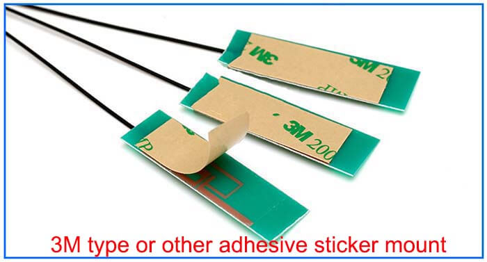
Below are the existing Flexible single-band & dual-band Wifi PCB Antenna Design styles for your choice.
18x7mm(Flex PCB Antenna) Mini Wifi Antenna Embedded Antenna FPC
30x14mm(Flex PCB Antenna) Flex PCB Antenne Wifi 2.4 GHz
40x6mm(Flex PCB Antenna) Internal 2.4 GHz Wireless Antenna
25x9mm(Flex PCB Antenna) Smallest Wifi antenna Dual Wifi Antenna
28x9mm(Flex PCB Antenna) Mini Wifi Antenna Dual-band Wifi Antenna
31×5.5mm(Flex PCB Antenna) Internal Dual-band Wifi Antenna For PC
33x9mm(Flex PCB Antenna) Internal FPC Antenna Dual-band Wifi Antenna
35x11mm(Flex PCB Antenna) Wifi Ddual-band 2.4 GHz 5GHz Antenna
37x10mm(Flex PCB Antenna) Internal FPC Antenna Wifi Double Antenna
40x17mm(Flex PCB Antenna) 2.4 and 5GHz Wifi Antenna FPC Antenna
40x18mm(Flex PCB Antenna) Embedded Antenna 2.4 5 GHz Antenna
41x3mm(Flex PCB Antenna) 2 4 ghz antenne
42x7mm(Flex PCB Antenna) Indoor Wifi Antenna 2.4 GHz 5GHz
42x12mm(Flex PCB Antenna) FPC Embedded Antenna 2.4 5 GHz Antenna
46x14mm(Flex PCB Antenna) Flex PCB Dual-band Wifi Antenna
47x14mm(Flex PCB Antenna) Dual Wifi 2.4 GHz And 5GHz Antenna
50x14mm(Flex PCB Antenna) Indoor Dual-band High-gain Antenna
32x10mm(Flex PCB Antenna) Ipex MHF4 2.4G/5G Wifi Antennas
Wifi PCB Antenna Design Guide
The ultimate purpose of an antenna is to radiate RF signals into free space, and this is where antenna design becomes very important, but wifi PCB antenna design depends heavily on the characteristics of the platform it is installed.
In addition, the antenna is sensitive to the surrounding environment, these reasons lead to many cases where the antenna is a unique design for each platform.
Since customers are not very clear about the factors considered in wifi PCB antenna design, here are some of our suggestions on antenna design for portable devices so that customers can better design their own circuits and PCBs to increase the chances of project success.
However, each project has its own characteristics, so there are still some issues that need specific analysis.
WiFi PCB antenna Design requirements for PCB layout wiring and structure
1. The form of the antenna and the antenna location and feed point size recommendations
The built-in antenna is often used in several forms, respectively, divided into the form of LDS antenna, chip antenna, and FPC antenna.
The form of the chip antenna is a unified specification. There is a fixed size. The position and size of the pad according to the specific specifications of the antenna are also fixed.
In addition, there are design guidelines for specific antenna types, such as clear space requirements around the antenna and equipment size recommendations.
If bullet form is used, we suggest customers use PIFA antenna as WiFi antenna form. According to our experience, the PIFA antenna success rate and performance are better.
Antenna RF feeds solder plate should be taken size 2×3mm, pad containing the surrounding area of ≥ 0.8mm under all levels of PCB without copper cloth. If the PIFA antenna, but also adds a 2×3mm ground pad, the distance between the two pads for 2mm.
The usual location of the antenna is at the top of the device, the top of the PCB start. All the layers in this area of the ground are cut off 2 to 3mm but belong to the antenna ground pads of that layer of the pad part to be retained.
2. Suggestions for matching circuit wiring
The topology of the antenna matching circuit is four pieces from the antenna and string to string to the test port or power amplifier. Do not lay the ground under the matching circuit and a 1.5mm area around the matching network.
The matching network is placed closer to the feeder panel (but not too close).
3. Microstrip line from WiFi module to antenna matching circuit
The signal transmission line from the WiFi module to the antenna matching circuit is a microstrip line with a 50ohm characteristic impedance.
To avoid module losses on the microstrip line, the module should be as close to the antenna as possible. Microstrip lines must be sized according to the specific PCB. No crossed wires are allowed to pass between the microstrip line and the ground.
4. Some other issues
Grounding: Good RF grounding is undoubtedly quite important for the wireless performance of the phone and shall follow several design principles as follows.
Try to make the outer area of the ground intact, not divided and destroyed (non-shielded within the part). This is particularly important for the area near the antenna.
Antenna current must be isolated from the noise current, if the antenna near the ground area is destroyed into incomplete, must be generated in the relevant area below a filler ground plane, and use the ground hole to sew up, so that it becomes a complete ground.
This area alignment must ensure that the antenna current only flows through the surface plane and must limit the noise current flow into the complete ground plane inside.
When using pre-production antennas, it is important to note that the characteristics depend on the connected ground plane. The manufacturer’s specifications can only be met if the ground plane is of the same size and shape as the manufacturer’s evaluation board.
In other cases, the user needs to measure the impedance of the pre-produced antenna under actual application conditions and match it to the required characteristic impedance.
5. The use of metallic components in the equipment housing
Do not use spraying or plating with metallic components on the surface of the housing. The metallic plating cannot achieve reliable grounding and will have a great impact on the antenna performance.
Do not use metal decorations near the antenna.
6. The use of pure metal structure parts
When using all-metal structure parts (such as a front panel or rear panel), please reserve multiple grounding points for the used parts, and the specific location of the grounding points will be determined by the antenna design company.
There should not be any grounded or ungrounded metal decorations, including plating and gold plating, above the antenna radiation area.
7. To the antenna reserved for the installation location of the consideration
The antenna should be installed away from metal objects. The antenna needs enough space to spread. If a chip antenna is used, then it needs to give enough clearance area and the corresponding size of the ground as required by the application guide.
If the antenna of pop-up LDS antenna design method is used, the bracket should be designed for the antenna, and the antenna is fixed on the bracket, while the bracket and PCB are then fixed, or no bracket is used, and the antenna is fixed on top of the housing.
Consider giving space and location for antenna installation when doing structure design, and consider adding a thermal fusion post to fix the antenna on the bracket or the housing where the antenna is to be installed.
8. Consider the layout of other modules and antenna relative position
For the speaker, camera, vibrator, LCD, battery, and other components and the relative position of the antenna, here are some general recommendations.
The antenna should be located away from the camera and flexible PCB.
The antenna should be at least 5 mm away from the battery.
The vibrator is to be kept away from the antenna.
a minimum distance of 2-4mm from the antenna to the shield (which can cause parasitic effects)
RF switches and amplifiers or duplexers should be as close as possible to the matching circuit area.
Wifi PCB Antenna Design Features
Wifi PCB antenna design applications

Reviews
There are no reviews yet.