Description
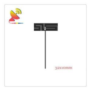
What is an Internal 2.4 GHz Antenna PCB Circuit Board Antenna?
The Internal 2.4 GHz Antenna PCB Circuit Board Antenna CTRF-ANTENNA-PCB-2450-3206-IPEX antenna item is an Internal 2.4 GHz Antenna PCB antenna Indoor Wi-Fi antenna manufactured by C&T RF Antennas Inc.
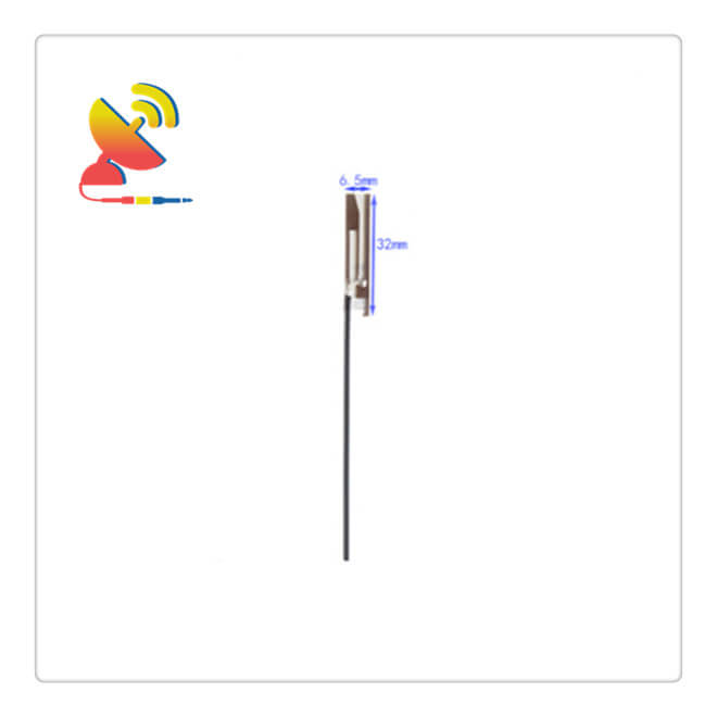
The Internal 2.4 GHz Antenna PCB Circuit Board Antenna comes with a 32×6.5mm small size 2dBi gain antenna with a U.FL/Ipex connector directly mounted to the terminal devices.
Internal 2.4 GHz Antenna PCB Circuit Board Antenna Features:
Easy mount
Compact size
High-performance
Stable signal
Internal 2.4 GHz Antenna PCB Circuit Board Antenna Is Available At C&T RF Antennas Inc. We provide the RF antennas with other antenna radio frequencies such as 169MHz, 230MHz, 315MHz, 433MHz, 868MHz, 915MHz, Lora, NFC, VHF&UHF, NB-IoT, ADS-B, GSM, Wifi 2.4GHz, 5.8GHz, 2G 3G 4G LTE, GPS, GNSS, 5G NR, UWB, Cellular, etc.
We provide indoor & outdoor wireless LAN antennas with many antenna types such as Dipole Antennas, Whip Antennas, Marine Antennas, Router Antennas, MIMO Antennas, Combo Antennas, PCB Antennas, FPC Antennas, Spring Antennas, Sector Antennas, Yagi Antennas, etc., for IoT & M2M industries.
Contact For More Details On The 2.4 GHz WiFi Circuit Board Antenna Such As The Circuit Board Antenna’s Datasheet, PCB Circuit Board Antenna Pricing, PCB Circuit Board Antenna inventory, or other frequency bands PCB Circuit Board Antenna.
Internal 2.4 GHz Antenna PCB Circuit Board Antenna Specifications
Internal 2.4 GHz Antenna PCB Circuit Board Antenna Electrical Specifications |
|
| RF Antenna Type | Embedded PCB Antenna |
| Model | CTRF-ANTENNA-PCB-2450-3206-IPEX |
| Frequency | 2400-2500 MHz |
| Gain | 2dBi |
| VSWR | ≤2.0 |
| Impedance | 50 Ω |
| Polarization | Vertical/Linear |
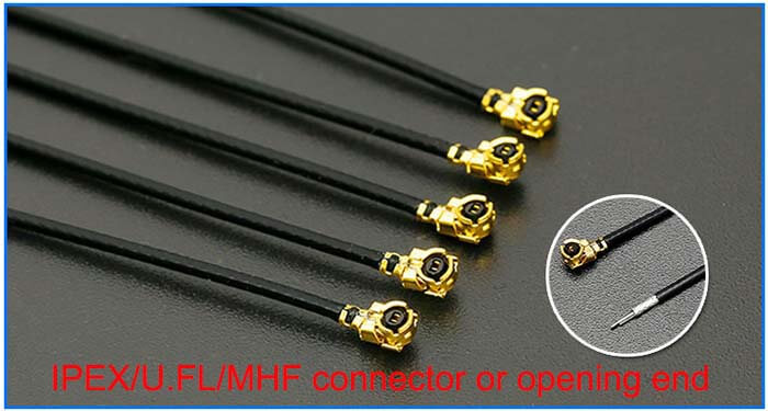
| Cable Type | RG1.13 |
| Connector | U.FL/IPEX |
| Cable Length | 100mm |
| Lightning Protection | DC-Ground |
Internal 2.4 GHz Antenna PCB Circuit Board Antenna Mechanical Specifications |
|
| PCB Board Dimension | 6.5*32m |
| Weight | Approx. 3g |
| Material | PCB |
| Operation Temperature | -40˚C ~ +85˚C |
| Storage Temperature | -40˚C ~ +80˚C |
| Color | White |
| Antenna Design | Dipole Array |
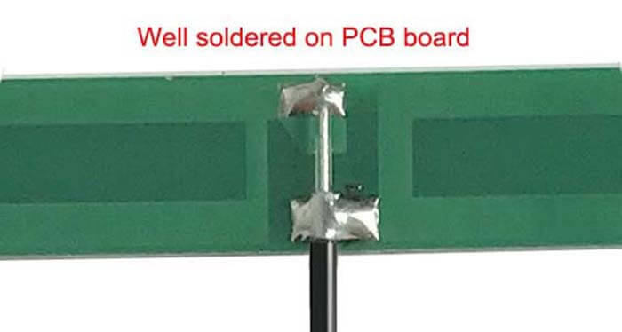
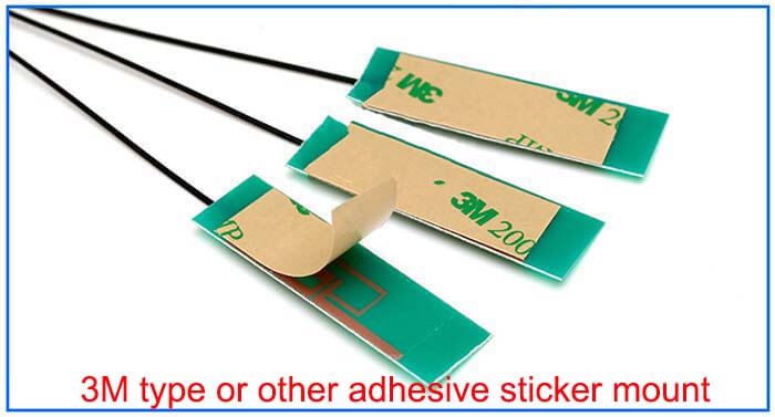
| Mounting | Connector/Sticker |
| Safety Emission and other | RoHS Compliant |
| Applications | ISM/SCADA/Utilities, IoT/M2M, WLAN/Wi-Fi/Bluetooth/Zigbee/Sigfox, etc |
2.4 GHz WiFi Circuit Board Antenna Features
Circuit Board Antenna Applications

What are the requirements of the WIFI antenna for the Circuit Board Antenna layout?
1. Antenna form, antenna position, and feed point size recommendations
The several forms that the built-in antennas often use are divided into shrapnel form, a chip patch antenna, a Circuit Board Antenna PCB antenna FPC antenna.
The form of the patch antenna is uniform and has a fixed size. The position and size of the pad are also fixed according to the specific specifications of the antenna.
In addition, according to the specific antenna model, there are relevant design guidelines such as the requirements for the clearance around the antenna and the suggestion of equipment size.
If using shrapnel form, we recommend that customers use a PIFA antenna as the form of a WiFi antenna. According to our experience, the success rate and performance of the PIFA antenna are better.
The size of the antenna RF feed pad should be 2&TImes, and 3mm, and no copper should be placed on all layers of the PCB with an area ≥of 0.8mm from the periphery of the pad. If it is a PIFA antenna, add a 2&TImes; a 3mm ground pad, and the distance between the two pads is 2mm.
The antenna is usually located on the top of the device, starting from the top of the PCB, cut off the ground of all layers in this area by 2 to 3 mm, but the pad part of the layer that belongs to the antenna ground pad should be kept.
2. Suggestions for matching circuit wiring
The topological structure of the antenna matching circuit is from the antenna to the test port or Power amplifier. Do not lay the ground under the matching circuit and in the 1.5mm area around the matching network. It is better to place the matching network closer to the feed pad (but not too close).
3. Microstrip line from WiFi module to antenna matching circuit
The signal transmission line from the WiFi module to the antenna matching circuit is a 50ohm characteristic impedance microstrip line.
In order to avoid loss on the microstrip line, the module should be as close as possible to the antenna. The size of the microstrip line must be determined according to the specific PCB. Crossing lines are not allowed to pass between the microstrip line and the ground.
4. Some other issues
Grounding: A good RF grounding is undoubtedly very important for the wireless performance of mobile phones. The following design principles must be followed:
Try to make the ground in the outer area as complete as possible and not be damaged by segmentation (the part inside the non-shielding cover). This is especially important for the area near the antenna. The antenna current must be isolated from the noise current.
If the grounding area near the antenna is destroyed to be incomplete, a filled ground plane must be created in the relevant area below it and stitched with ground vias to make it a complete ground.
The wiring in this area must ensure that the antenna current only flows through the surface plane, and the noise current must be restricted from flowing into the complete ground plane inside.
When using a pre-produced antenna, it should be noted that its characteristics depend on the connected ground plane. Only when the size and shape of the ground plane are consistent with the manufacturer’s evaluation board, can the manufacturer’s marked specifications be reached.
In other cases, the user needs to measure the impedance of the pre-produced antenna under actual application conditions and match it to the required characteristic impedance.
5. The use of metal components in the equipment shell
Do not use spraying or plating with metal components on the surface of the shell. The metal plating cannot achieve reliable grounding, which will have a great impact on the antenna performance.
Do not use metal decorations near the antenna.
6. Use of pure metal structural parts
When using all-metal components (such as the front panel or the rear panel), please reserve multiple grounding points for the components used. The specific grounding point location is determined by the antenna design company.
There should be no grounded or ungrounded metal decorations above the antenna radiation area, including electroplating and gold plating.
7. Consideration of reserving installation location for the antenna
The antenna should be installed far away from metal objects, and the antenna needs enough space to unfold. If a chip antenna is used, then it is necessary to provide sufficient clearance area and ground of the corresponding size in accordance with the requirements of the application guide.
If a shrapnel antenna is used, support should be designed for the antenna, and the antenna should be fixed on the support, and the support and PCB should be fixed; or without the support, the antenna should be fixed on the shell.
When designing the structure, consider the space and location of the antenna installation, and consider adding a hot-melt column to the bracket or the shell where the antenna is to be installed to fix the antenna.
8. Consideration of the relative position layout of other modules and antennas
For the relative position of the speaker, camera, vibrator, LCD, battery and other components, and the antenna, here are some general suggestions:
The antenna should be far away from the camera and flexible PCB;
The antenna must be at least 5mm away from the battery;
Keep the Vibrator away from the antenna;
The minimum distance between the antenna and the shield is 2-4mm (which will cause parasitic effects);
RF switches and amplifiers or duplexers should be as close as possible to the matching circuit area.
Reviews
There are no reviews yet.