Description
Who provides 2.4 GHz Bluetooth Antenna Internal PCB Antenna Design?
The 2.4 GHz Bluetooth Antenna Internal PCB Antenna Design service is supplied by C&T RF Antennas Inc., the embedded PCB antenna and flexible PCB antenna design and manufacturer in China.
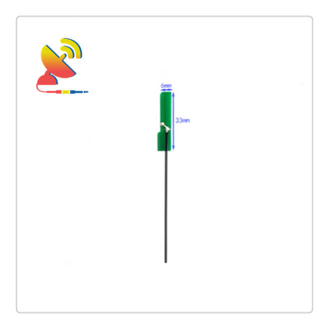
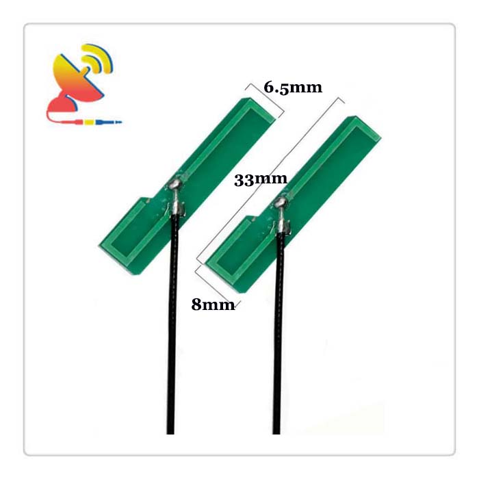
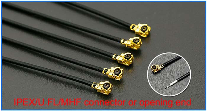
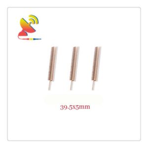
The embedded antenna item is a 2.4 GHz Bluetooth Antenna CTRF-ANTENNA-PCB-2450-3306-IPEX antenna model with Internal PCB Antenna Design 33×6.5mm small size PCB circuit board antenna with Ipex/U.FL connector antenna directory mounts to smart devices for IoT and M2M industries.
2.4 GHz Bluetooth Antenna Internal PCB Antenna Design Features:
Embedded antenna
Coaxial cable antenna
Ipex connector antenna
2.4G frequency
Wifi, wireless, Bluetooth, Zigbee, etc
High antenna radiation performance
Combines greater space savings with secure mounting to the application device chassis
Ensures robust antenna reliability and connectivity to the radio device
Reduces engineering resources and costs needed to mitigate PCB ground-induced radiation
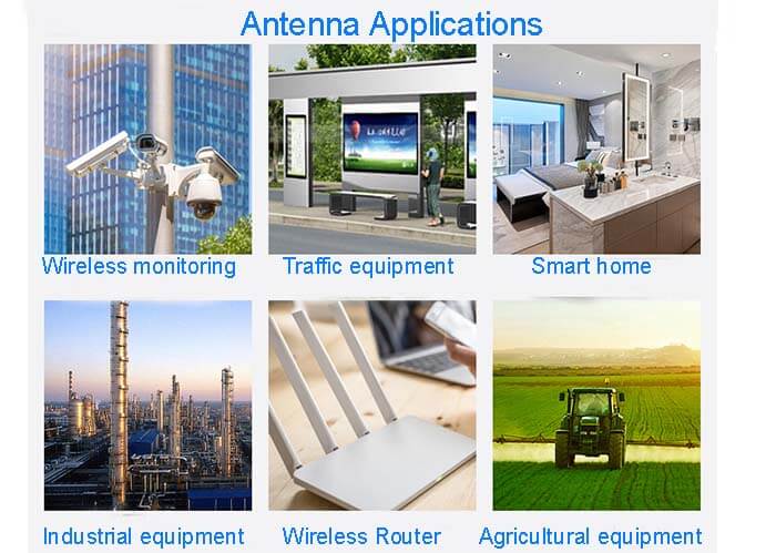
Suitable antenna for IoT applications
A wide selection of micro-coaxial cable lengths from 50 to 300mm
Extends connectivity for maximum design flexibility
The 2.4 GHz Bluetooth Antenna Internal PCB Antenna Design Is Available At C&T RF Antennas Inc., Contact Us For The Bluetooth Antenna Design.
C&T RF Antennas Inc provides RF antennas with other antenna radio frequencies such as 169MHz, 230MHz, 315MHz, 433MHz, 868MHz, 915MHz, Lora, NFC, VHF&UHF, NB-IoT, ADS-B, GSM, Wifi 2.4GHz, 5.8GHz, 2G 3G 4G LTE, GPS, GNSS, 5G NR, UWB, Cellular, etc.
We provide indoor & outdoor wireless LAN antennas with many antenna types such as Dipole Antennas, Whip Antennas, Marine Antennas, Router Antennas, MIMO Antennas, Combo Antennas, PCB Antennas, FPC Antennas, Spring Antennas, Sector Antennas, Yagi Antennas, etc., for IoT & M2M industries.
Welcome your original ideas to do the PCB antenna design such as Lora PCB antenna design, NB-IoT PCB antenna design LTE PCB antenna design, GSM 3G PCB antenna design, wifi PCB antenna design, 5G NR PCB antenna design, etc.
2.4 GHz Bluetooth Antenna Internal PCB Antenna Design Specifications
2.4 GHz Bluetooth Antenna Internal PCB Antenna Design Electrical Specifications |
|
| RF Antenna Type | Embedded PCB Antenna |
| Model | CTRF-ANTENNA-PCB-2450-3306-IPEX |
| Frequency | 2400-2500 MHz |
| Gain | 2dBi |
| VSWR | ≤2.0 |
| Impedance | 50 Ω |
| Polarization | Vertical/Linear |
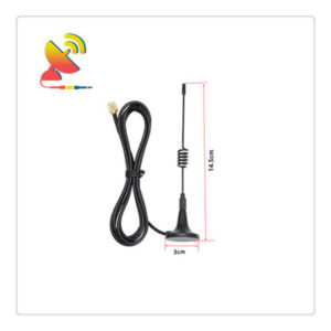
| Cable Type | RG1.13 |
| Connector | U.FL/IPEX |
| Cable Length | 130mm |
| Lightning Protection | DC-Ground |
2.4 GHz Bluetooth Antenna Internal PCB Antenna Design Mechanical Specifications |
|
| PCB Board Dimension | 33*6.5mm |
| Weight | Approx. 3g |
| Material | PCB |
| Operation Temperature | -40˚C ~ +85˚C |
| Storage Temperature | -40˚C ~ +80˚C |
| Color | Green |
| Antenna Design | Dipole Array |
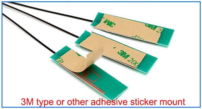
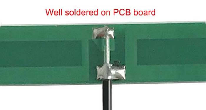
| Mounting | Connector/Sticker |
| Safety Emission and other | RoHS Compliant |
| Applications | ISM/SCADA/Utilities, IoT/M2M, WLAN/Wi-Fi/Bluetooth/Zigbee/Sigfox, etc. |
2.4 GHz Bluetooth PCB Antenna Drawing
PCB Antenna Design Features
PCB Antenna Design Applications
Four major Bluetooth antenna design methods
For a long time, whether it is a smartphone, a laptop, or a tablet, Bluetooth has been the standard configuration of smart devices.
With the development of the mobile Internet, a large number of smart wearable devices are now emerging, and supporting the development of these applications requires not only the support of mobile software but also the support of wireless sensing technology.
Bluetooth is still the preferred communication method for wireless connections.
Bluetooth technology is the most important link in the middle. Not only requires communication sensitivity, but also requires miniaturization, low power consumption, and more importantly, low cost.
The appearance of the Bluetooth 4.0 version solves these problems, it includes Bluetooth Smart (low power consumption) function, and has the following characteristics:
1) Low energy consumption
2) Low cost
3) Standard button batteries can run the equipment for several years
4) Multi-vendor interoperability
5) Enhanced range
In the hardware design, the antenna design is more particular. The commonly used low-cost design method is the PCB onboard antenna design method, but how should the PCB onboard antenna be designed in practice to achieve a good transmission and reception effect? There are four Bluetooth antenna designs below for reference.
Inverted F antenna for Bluetooth antenna design
The antenna body of the inverted-F antenna can be linear or sheet-shaped, and the size of the Bluetooth antenna can be reduced when an insulating material with a higher dielectric constant is used.
As a kind of onboard antenna, the inverted F antenna has a low design cost but adds a certain volume, and is the most common one in practical applications.
The antenna is generally placed on the top layer of the PCB, and the ground is generally placed on the top layer and near the antenna, but the ground must not be placed around the antenna, and the surrounding area should be a clear space.
Meander antenna design of Bluetooth antenna design
The length of a meander antenna is more difficult to determine. The length is generally slightly longer than a quarter-wavelength, and its length is determined by its geometric topological space and area.
The meander antenna is generally a PCB package, that is, an onboard antenna. Like the inverted F type, the antenna is generally placed on the top layer of the PCB, and the ground is generally placed on the top layer and near the antenna, but the ground must not be placed around the antenna, and the surrounding area should be a clear space.
Note: The antenna length calculation formula:
The length of the antenna (m)=(300/f)*0.25*0.96
Where f is the frequency (MHz), 0.96 is the wavelength shortening rate
The length of the Bluetooth antenna is about 300/2.4G*0.25*0.96, which is about 31mm
Ceramic antenna design of Bluetooth antenna design
The ceramic antenna is another miniaturized antenna suitable for Bluetooth devices. The types of ceramic antennas are divided into bulk ceramic antennas and multilayer ceramic antennas. Since the dielectric constant of the ceramic itself is higher than that of the PCB circuit board, the use of ceramic antennas can effectively reduce the size of the antenna.
In terms of dielectric loss, the ceramic medium is also smaller than the dielectric loss of the PCB circuit board, so it is very suitable for low power consumption Used in the Bluetooth module.
When designing the PCB, it is sufficient to have a clear space around the antenna and pay special attention to not applying copper.
2.4G rubber duck antenna design of Bluetooth antenna design
The 2.4G rod-shaped rubber duck antenna Bluetooth antenna is a little bit large, but the transmission distance is stronger than other antennas. When designing the PCB, there should be clearance around the antenna as with the above three antenna designs.
Other relevant notes about Bluetooth antenna design:
1) The antenna’s signal (frequency greater than 400MHz) is easily attenuated, so the distance between the antenna and the nearby ground should be at least three times the line width.
2) For microstrip lines and strip lines, the characteristic impedance is related to the thickness, line width, vias, and dielectric constant of the board.
3) Vias will produce parasitic inductance, and high-frequency signals will have very large attenuation, so try not to have vias when routing RF lines.
Reviews
There are no reviews yet.