What is radio frequency power amplifier?
The radio frequency power amplifier (RF Power Amplifier or RF PA) is the main part of the transmitting system, and its importance is self-evident.
In the pre-stage circuit of the transmitter, the RF signal power generated by the modulation oscillator circuit is very small, and it needs to go through a series of amplification (buffer stage, intermediate amplification stage, final power amplification stage) to obtain enough RF power before it can be fed Radiate to the antenna.
In order to obtain a large enough radio frequency output power, a radio frequency power amplifier must be used. After the modulator generates the radio frequency signal, the radio frequency modulated signal is amplified to sufficient power by the radio frequency power amplifier and then transmitted by the antenna through the matching network.
The function of the amplifier is to amplify the input content and output it. The content of input and output, which we call signals, is often expressed as voltage or power.
For a system such as an amplifier, its contribution is to raise what it absorbs to a certain level and output it to the outside world. If the amplifier can have good performance, then it can contribute more, which reflects its own value.
If the amplifier has certain problems, not only can it no longer provide any contribution after it has started or has been working for a period of time, but some oscillations may occur. Such oscillations are disastrous for the outside world or the amplifier itself.
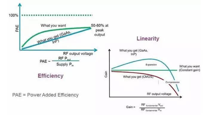
The main technical indicators of radio frequency power amplifiers are output power and efficiency. How to improve output power and efficiency is the core of the design goals of radio frequency power amplifiers.
Usually, in a radio frequency power amplifier, an LC resonant circuit can be used to select the fundamental frequency or a certain harmonic to achieve distortionless amplification. In addition, the harmonic components in the output should be as small as possible to avoid interference with other channels.
Radio Frequency Power Amplifier classification
According to different working conditions, power amplifiers are classified as follows:
Working status is classified into Class A amplifier, Class B amplifier, Class C amplifier, Class D amplifier, Class E amplifier, Class F amplifier.
Among them, the linear power amplifier has
Switching power amplifier has
Class D power amplifier
Class E power amplifier
Class F power amplifier
The operating frequency of traditional linear power amplifiers is very high, but the relative frequency band is relatively narrow. Radiofrequency power amplifiers generally use frequency selective networks as load loops.
Radio frequency power amplifiers can be divided into three types of working states: A, B, and C according to the current conduction angle.
The conduction angle of the class A amplifier current is 360°, which is suitable for small signal low-power amplification. The conduction angle of the class B amplifier current is equal to 180°, and the conduction angle of the class C amplifier current is less than 180°.
Both Class B and Class C are suitable for high-power working conditions, and the output power and efficiency of Class C working conditions are the highest among the three working conditions.
Most radio frequency power amplifiers work in Class C, but the current waveform distortion of Class C amplifiers is too large and can only be used to amplify the resonant power of the load by using a tuning loop. Due to the filtering capability of the tuning loop, the loop current and voltage are still close to sinusoidal waveforms, and the distortion is small.
Switching Mode PA (SMPA) makes electronic devices work in a switching state. Commonly used are Class D amplifiers and Class E amplifiers. Class D amplifiers are more efficient than Class C amplifiers.
SMPA drives active transistors in switch mode. The working state of the transistors is either on or off. There is no overlap in the time-domain waveforms of voltage and current, so the DC power consumption is zero, and the ideal efficiency can reach 100 %.
Traditional linear power amplifiers have high gain and linearity but low efficiency while switching power amplifiers have high efficiency and high output power, but poor linearity.
Circuit composition
There are different types of amplifiers. To simplify, the amplifier circuit can be composed of the following parts, transistors, bias and stabilization circuits, and input and output matching circuits.
Transistor
There are many kinds of transistors, including many other types of transistors that have been invented. Essentially, the work of a transistor is expressed as a controlled current source or voltage source, and its working mechanism is to convert the energy of direct current without content into a useful output. DC energy is obtained from the outside world, consumed by transistors, and converted into useful components.
Different transistors have different capabilities, such as their ability to withstand the power. This is also due to their different ability to obtain DC energy; for example, their response speed is different, which determines how wide and high the frequency band can work. For example, the impedance of the input and output terminals is different, and the ability to react to the outside is different, which determines the difficulty of matching it.
Bias circuit and stabilization circuit
Bias and stabilization circuits are two different circuits, but because they are often difficult to distinguish and the design goals are the same, they can be discussed together.
The operation of the transistor needs to be under certain bias conditions, which we call the static operating point. This is the basis of the transistor’s foothold and its own positioning.
Each transistor has a certain positioning for itself, and its different positioning will determine its own working mode, and there are also different performances in different positioning.
Some positioning points have small fluctuations, which are suitable for small signal work;
Some positioning points have large fluctuations, which are suitable for high-power output; some positioning points require less demand, pure release, and are suitable for low-noise work;
At some positioning points, the transistor is always hovering between saturation and cut-off, in a switching state.
An appropriate bias point is a basis for normal operation. When designing a broadband power amplifier, or when the operating frequency is high, the bias circuit has a greater impact on the circuit performance. At this time, the bias circuit should be considered as a part of the matching circuit.
There are two types of bias networks, passive networks, and active networks.
Passive networks (ie, self-biased networks) are usually composed of resistor networks to provide suitable operating voltage and current for the transistors. Its main drawback is that it is very sensitive to changes in transistor parameters and has poor temperature stability.
The active bias network can improve the stability of the static operating point and also improve the good temperature stability, but it also has some problems, such as increasing the circuit size, increasing the difficulty of circuit layout, and increasing power consumption.
The stabilization circuit must be before the matching circuit because the transistor needs to have the stabilization circuit as a part of itself, and then contact the outside world. From the outside world, the transistor with the stability circuit is a brand-new transistor. It made certain sacrifices and gained stability. The mechanism of stabilizing the circuit can ensure the smooth and stable operation of the transistor.
Input and output matching circuit
The purpose of the matching circuit is to choose an acceptable method. For those transistors that want to provide greater gain, the way is to accept and output the whole.
This means that through the interface of the matching circuit, the communication between different transistors is smoother. For different types of amplifiers, the matching circuit is not the only way to accept a design.
Some small tubes with small DC and shallow foundations are more willing to make a certain block when they accept it to obtain better noise performance. However, they cannot block too much, otherwise, their contribution will be affected.
For some giant power tubes, you need to be cautious when outputting, because they are more unstable, and at the same time, certain retention helps them to exert more undistorted energy.
Typical impedance matching networks include L-matching, π-shaped matching, and T-shaped matching. Among them, L matching is characterized by a simple structure and only two degrees of freedom L and C.
Once the impedance conversion ratio and resonance frequency are determined, the Q value (bandwidth) of the network is also determined.
One of the advantages of the π-shaped matching network is that no matter what kind of parasitic capacitance is connected to it, it can be absorbed into the network. This also leads to the general application of the π-shaped matching network, because in many practical situations, it is dominant. The parasitic element of the position is capacitance.
When the parasitic parameters of the power supply terminal and the load terminal are mainly inductive, T-shaped matching can be used to absorb these parasitic parameters into the network.
The way to ensure the stability of radio frequency power amplifier
Every transistor is potentially unstable. A good stable circuit can be integrated with the transistor to form a sustainable working model.
The realization of the stabilization circuit can be divided into two types, narrowband and broadband.
The narrow-band stabilization circuit performs certain gain consumption. This kind of stabilization circuit is realized by adding a certain consumption circuit and a selective circuit.
This kind of circuit makes the transistor can only contribute in a small frequency range. Another kind of broadband stabilization is the introduction of negative feedback. This circuit can work in a wide range.
The source of instability is positive feedback, and the narrow-band stabilization idea is to suppress a part of the positive feedback, which also suppresses the contribution.
And the negative feedback is done well, and there are many extra gratifying advantages. For example, negative feedback may prevent the transistor from being matched, and it can communicate well with the outside world without matching.
In addition, the introduction of negative feedback will improve the linear performance of the transistor.
The efficiency improvement technology of radio frequency power amplifier
The efficiency of transistors has a theoretical limit. This limit varies with the selection of the bias point (static operating point). In addition, poorly designed peripheral circuits will greatly reduce their efficiency. At present, there are not many ways for engineers to improve efficiency. Here are only two, envelope tracking technology and Doherty technology.
The essence of envelope tracking technology is:
The input is separated into two types, phase, and envelope, and then amplified by different amplifying circuits. In this way, the two amplifiers can focus on their respective parts, and the cooperation of the two can achieve the goal of higher efficiency utilization.
The essence of Doherty technology is:
Two transistors of the same type are used, and only one works at small input and works in a high-efficiency state. If the input increases, the two transistors work at the same time. The basis of this method is that the two transistors must cooperate with each other tacitly. The working state of one kind of transistor will directly determine the working efficiency of the other.
Test Challenges Faced by radio frequency power amplifier
Radio frequency power amplifiers are very important components in wireless communication systems, but they are non-linear in themselves, which can cause spectrum proliferation and interfere with adjacent channels, and may violate out-of-band emission standards mandated by laws and regulations.
This feature can even cause in-band distortion, which causes the bit error rate (BER) of the communication system to increase and the data transmission rate to decrease.
Under the peak-to-average power ratio (PAPR), the new OFDM transmission format will have more occasional peak power, making the radio frequency power amplifier difficult to be divided. This will reduce the compliance of the spectrum mask and expand the EVM of the entire waveform and increase the BER.
In order to solve this problem, design engineers usually deliberately reduce the operating power of the radio frequency power amplifier. Unfortunately, this is a very inefficient method, because the PA reduces the operating power by 10% and loses 90% of the DC power.
Most radio frequency power amplifiers nowadays support multiple modes, frequency ranges, and modulation modes, making the test items more numerous. Thousands of test items are not uncommon.
The application of new technologies such as crest factor reduction (CFR), digital predistortion (DPD), and envelope tracking (ET) can help optimize PA performance and power efficiency, but these technologies will only make the test more complicated and extend significantly Design and test time.
Increasing the bandwidth of the radio frequency power amplifier will increase the bandwidth required for DPD measurement by 5 times (maybe more than 1 GHz), resulting in a further increase in test complexity.
According to the trend, in order to increase efficiency, radio frequency power amplifier components and front-end modules (FEM) will be more closely integrated, and a single FEM will support a wider range of frequency bands and modulation modes. Integrating the envelope tracking power supply or modulator into the FEM can effectively reduce the overall space requirement inside the mobile device.
In order to support a larger operating frequency range, a large number of filter/duplexer slots are added, which will increase the complexity of mobile devices and the number of test items.
Changes in semiconductor materials:
Ge (germanium), Si (silicon) → GaAs (gallium arsenide), InP (indium phosphide) → SiC (silicon carbide), GaN (gallium nitride), SiGe (silicon germanium), SOI (overlay of insulating layer) (Silicon) → Carbon Nanotube (CNT) → Graphene (Graphene).
At present, the mainstream process of power amplifiers is still the GaAs process. In addition, GaAs HBT, gallium arsenide heterojunction bipolar transistor. Among them, HBT (heterojunction bipolar transistor) is a bipolar transistor composed of a gallium arsenide (GaAs) layer and an aluminum gallium arsenide (AlGaAs) layer.
Although the CMOS process is relatively mature, the application of Si CMOS power amplifiers is not extensive.
In terms of cost, although the CMOS process silicon wafer is relatively cheap, the CMOS power amplifier layout area is relatively large, coupled with the high research and development costs invested in the complex design of CMOS power amplifier, the overall cost advantage of CMOS power amplifiers is not so obvious.
In terms of performance, CMOS power amplifiers have poor performance in terms of linearity, output power, efficiency, etc., coupled with the inherent shortcomings of CMOS technology, high knee voltage, low breakdown voltage, and resistance of CMOS technology substrates The rate is low.
Carbon nanotubes (CNT) are considered to be ideal materials for nanoelectronic devices due to their small physical size, high electron mobility, high current density, and low intrinsic capacitance.
The zero bandgap semiconductor material graphene, because of its high electron migration rate, nano-scale physical size, excellent electrical and mechanical properties, will surely become a popular material for the next generation of radio frequency chips.
Linearization technology of radio frequency power amplifier
The non-linear distortion of the radio frequency power amplifier will cause it to generate new frequency components. For example, the second-order distortion will produce the second harmonic and two-tone beat frequency. For the third-order distortion, it will produce the third harmonic and multi-tone beat frequency.
If these new frequency components fall within the passband, they will cause direct interference to the transmitted signal, and if they fall outside the passband, they will interfere with other channels’ signals.
For this reason, it is necessary to linearize the radio frequency power amplifier, which can better solve the problem of signal spectrum regeneration.
The principle and method of the basic linearization technology of the radio frequency power amplifier is nothing more than taking the amplitude and phase of the input RF signal envelope as a reference, comparing it with the output signal, and then generating appropriate corrections.
Currently, the power amplifier linearization techniques that have been proposed and widely used include power back-off, negative feedback, feedforward, predistortion, envelope elimination and recovery (EER), and linear amplification using nonlinear elements (LINC).
More complex linearization techniques, such as feedforward, predistortion, envelope elimination, and restoration, use nonlinear elements for linear amplification, and they have a better effect on improving the linearity of the amplifier.
Realization of relatively easy linearization techniques, such as power back-off, negative feedback, these techniques have limited improvement in linearity.
Power fallback
This is the most commonly used method, which is to use a larger power tube as a small power tube, in fact, at the expense of DC power consumption to improve the linearity of the radio frequency power amplifier.
The power back-off method is to compress the input power of the radio frequency power amplifier from the 1dB compression point (the amplifier has a linear dynamic range, within this range, the output power of the amplifier increases linearly with the input power.
As the input power continues to increase, the radio frequency power amplifier gradually enters the saturation region, and the power gain begins to decrease. The output power value when the gain drops to 1dB lower than the linear gain is usually defined as the 1dB compression point of the output power, which is represented by P1dB.
Backward 6-10 decibels, working at a level far less than the 1dB compression point, so that the power amplifier is far away from the saturation zone and enters the linear working zone, thereby improving the third-order intermodulation coefficient of the radio frequency power amplifier.
In general, when the fundamental wave power is reduced by 1dB, the third-order intermodulation distortion is improved by 2dB.
The power back-off method is simple and easy to implement and does not require any additional equipment. It is an effective method to improve the linearity of the amplifier. The disadvantage is that the efficiency is greatly reduced.
In addition, when the power falls back to a certain level when the third-order intermodulation reaches below -50dBc, continuing to fall back will no longer improve the linearity of the amplifier. Therefore, it is not enough to rely solely on power back-off on occasions where the linearity requirements are very high.
Predistortion
Predistortion is to add a non-linear circuit in front of the radio frequency power amplifier to compensate for the non-linear distortion of the radio frequency power amplifier.
The advantages of predistortion linearization technology are that there is no stability problem, a wider signal frequency band, and the ability to process signals with multiple carriers.
The cost of predistortion technology is low. Several carefully selected components are packaged into a single module and connected between the signal source and the power amplifier to form a predistortion linear power amplifier.
The radio frequency power amplifier in the handheld mobile station has adopted the predistortion technology, which reduces the intermodulation products by a few dB with only a few components, but it is a critical few dB.
Pre-distortion technology is divided into two basic types: RF pre-distortion and digital baseband pre-distortion.
RF predistortion is generally implemented by analog circuits, which have the advantages of simple circuit structure, low cost, easy high-frequency, broadband applications, etc. The disadvantage is that the spectrum regeneration component is less improved and the high-order spectrum components are more difficult to cancel.
Digital baseband predistortion can be realized by digital circuits due to their low operating frequency. It has strong adaptability. It can also offset high-order intermodulation distortion by increasing the sampling frequency and increasing the quantization order. It is a promising method.
This predistorter is composed of a vector gain adjuster, which controls the amplitude and phase of the input signal according to the content of the look-up table (LUT), and the magnitude of the predistortion is controlled by the input of the look-up table.
Once the vector gain regulator is optimized, it will provide a non-linear characteristic opposite to that of a radio frequency power amplifier.
Ideally, the output intermodulation product at this time should be equal to the output amplitude of the dual-tone signal through the power amplifier but opposite in phase, that is, the adaptive adjustment module is to adjust the input of the look-up table, so as to minimize the difference between the input signal and the output signal of the radio frequency power amplifier.
Note that the envelope of the input signal is also an input of the lookup table. The feedback path samples the distortion output of the radio frequency power amplifier, and then sends it to the adaptive adjustment DSP through A/D conversion to update the lookup table.
Feed-forward
Feed-forward technology originated from feedback. It is not a new technology. It was proposed by Bell Labs in the United States as early as the 1920s and 1930s. Except for calibration (feedback) which is added to the output, it is completely feedback in concept.
The feed-forward linear amplifier forms two loops through the coupler, attenuator, synthesizer, delay line, power divider, etc.
After the RF signal is input, it is divided into two channels by the power divider. All the way into the main power amplifier, due to its nonlinear distortion, in addition to the main frequency signal that needs to be amplified, there is also third-order intermodulation interference at the output.
A part of the signal is coupled from the output of the main power amplifier, and the main carrier frequency signal of the amplifier is canceled by loop 1, leaving only the inverted third-order intermodulation component.
After the third-order intermodulation component is amplified by the auxiliary amplifier, it cancels the intermodulation component generated by the nonlinearity of the main amplifier through 2 loops, thereby improving the linearity of the radio frequency power amplifier.
Feed-forward technology not only provides the advantages of higher calibration accuracy but also does not have the disadvantages of instability and limited bandwidth. Of course, these advantages are exchanged for the high cost. Because of the high power level during output calibration, the calibration signal needs to be amplified to a higher power level. This requires an additional auxiliary amplifier and requires the auxiliary amplifier itself. The distortion characteristic should be above the index of the feed-forward system.
The cancellation requirements of the feed-forward power amplifier are very high, and the matching of amplitude, phase, and time delay needs to be obtained. If power changes, temperature changes, and device aging, etc. occur, the cancellation will disappear. For this reason, consider the adaptive cancellation technology in the system, so that the cancellation can keep up with changes in the internal and external environments.
C&T RF Antennas Inc is the radio frequency power amplifier supplier in China, we provide the UHF radio frequency power amplifiers, VHF radio frequency power amplifiers, Wifi radio frequency power amplifiers, 5GHz radio frequency power amplifiers, LTE radio frequency power amplifiers, GSM radio frequency power amplifiers, etc.
Contact us for more details on radio frequency power amplifiers.
You may also be interested in the below articles.
What is the difference between WIFI and WLAN?
Summary of 41 Basic Knowledge of LTE
What Are The Advantages And Characteristics Of NB-IoT And LoRa?