
This A Complete Guide For PCB 2.4G Antenna Design article introduces the design of the antenna and recommends two tested low-cost PCB antennas. These PCB 2.4G antenna designs can be used with Bluetooth Low Energy (BLE) solutions. For the best performance, BLE and BLE 2.4GHz radio frequencies must be correctly matched to their antennas.
1. PCB 2.4G Antenna Design Introduction
The antenna is a key component in the wireless system, and it is responsible for sending and receiving electromagnetic radiation from the air.
Designing antennas for low-cost, consumer-wide applications and integrating them into portable products is a challenge that most original equipment manufacturers (OEMs) are facing.
The wireless range that the end customer obtains from a certain RF product (such as a coin-type battery with limited power) mainly depends on the design of the antenna, the plastic casing, and a good PCB layout.
For systems with the same chip and power supply but different layout and antenna design practices, it is normal for their RF (radio frequency) range to vary by more than 50%.
This application note introduces best practices, layout guidelines, and antenna tuning procedures, and gives the widest band that can be obtained with a given amount of power.
A well-designed antenna can expand the working range of wireless products. The greater the energy sent from the wireless module, the greater the transmission distance under the conditions of the given packet error rate (PER) and the fixed receiver sensitivity.
In addition, antennas have other less obvious advantages. For example, a well-designed antenna can emit more energy within a given range, thereby improving error tolerance (caused by interference or noise). Similarly, a good debugging antenna and Balun (balancer) at the receiving end can work under extremely small radiation conditions.
The best antenna can reduce PER and improve communication quality. The lower the PER, the fewer retransmissions will occur, which can save battery power.
2. Antenna principle of PCB 2.4G Antenna Design
An antenna generally refers to a conductor that is exposed in space. When the length of the conductor is in a specific ratio or an integer multiple of the signal wavelength, it can be used as an antenna. Because the power supplied to the antenna is emitted into space, this condition is called resonance.
The wavelength of the conductor is λ/2, where λ is the wavelength of the electrical signal. The signal generator supplies power at the center of the antenna through a transmission line (also called an antenna feeder). According to this length, voltage and current standing waves will be formed on the entire wire.
The electrical energy input to the antenna is converted into electromagnetic radiation and radiated into the air at the corresponding frequency. The antenna is powered by the antenna feed, the characteristic impedance of the feed is 50Ω, and it radiates into space with a characteristic impedance of 377Ω.
Therefore, regarding the geometry of the antenna, there are two very important things to note:
A. Antenna length
B. Antenna feed
An antenna with a length of λ/2 is called a dipole antenna. However, in printed circuit boards, most of the conductors used as antennas are only λ/4 in length, but they still have the same performance.
By placing a ground plane at a certain distance below the conductor, a mirror image (λ/4) of the same length as the conductor can be created. When combined, these pins act as dipole antennas. This type of antenna is called a quarter-wavelength (λ/4) antenna.
Almost all antennas on the PCB are implemented in the size of a quarter wavelength on the copper ground plane. Note that the signal is now a single-ended feed, and the ground plane is used as the return path.
For the quarter-wavelength antennas used in most PCBs, special attention is required:
A. Antenna length
B. Antenna feed
C. The shape and size of the ground plane and return path
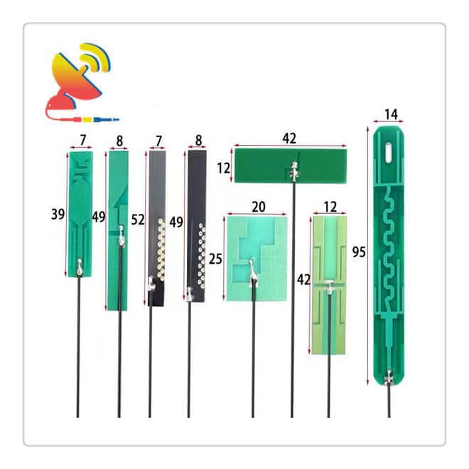
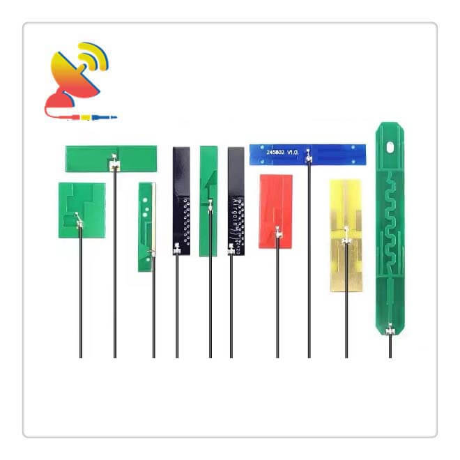
3. PCB 2.4G Antenna Design Types
As mentioned in the previous section, all conductors with a wavelength of λ/4 exposed in free space are placed on a ground plane and provided with a suitable voltage, then the conductor can be used as an antenna. Depending on the wavelength, the antenna may be as long as the FM antenna of a car, or as short as the trace on the signal buoy. For 2.4GHz applications, most PCB antennas belong to the following types.
3.1. Wire Antenna 2.4G Antenna Design
This is a section of wire extending into the free space on the PCB, its length is λ/4, and it is placed on the ground plane. This antenna is powered by a 50Ω impedance transmission line.
Generally, the wire antenna provides the best performance and radiation range. The wire can be straight, spiral, or looped. It is a three-dimensional (3D) structure in which the antenna is 4-5mm higher than the PCB and extends into space.
The wire antenna is a traditional old-style antenna. An aluminum wire or a quarter-wavelength paper clip is fixed on the PCB to form this antenna. The aluminum wire or paper clip is installed on the PCB in a spiral shape, and then 5 positions of -6mm are parallel to this layer.
Since they are exposed in the air as 3D antennas, their RF performance is very good. This antenna has the best signal range and the most isotropic radiation pattern. The wireless coverage of the wire antenna can exceed 100 feet.
For BLE applications that require a small form factor antenna, this type of antenna is not recommended because it will take up a lot of space and vertical height. But if there is enough space, this kind of antenna can achieve the best radio frequency range, directivity, and radiation pattern performance.
The wire antenna has the best radio frequency performance. Compared with other antennas, wire antennas have the best antenna gain and radiation performance.
3.2. PCB Antenna 2.4G Antenna Design
It is a PCB trace on the PCB, and it can be drawn as a straight trace, an inverted F-shaped trace, a serpentine or circular trace, etc. In a PCB antenna, unlike the wire antenna, the antenna is not exposed to the external space but exists in a two-dimensional (2D) structure on the same PCB layer.
When the 3D antenna exposed to space is placed on the PCB layer as a 2D PCB trace, certain guidelines must be followed. In general, compared with wire antennas, it requires more PCB space, low efficiency, but low cost, and can provide BLE applications with a receivable wireless distance.
3.3. Chip Antenna 2.4G Antenna Design
This is an antenna with a conductor. The antenna and conductor are assembled in a small IC package. When the antenna is packaged in a small size, it becomes very advantageous. Applications such as antenna USB nano transceivers will use this antenna when there is not enough space on the PCB to layout the PCB antenna.
For niche applications with very small PCB sizes (such as Bluetooth transceivers), chip antennas are a good way. They are off-the-shelf antennas, occupy the smallest PCB space, and can provide better performance. However, the chip antenna increases the bill of materials (BOM) and requires assembly costs. Because it requires ordering and assembly of external components.
When using a chip antenna, another key factor should also be considered, which is affected by the radiation ground area. Therefore, the manufacturer’s recommendation for the grounding area must be followed. Unlike PCB antennas, chip antennas cannot be adjusted by changing the antenna length. In addition, a matching network is required to adjust the antenna, so more bills of materials will be added.
For most applications, PCB antennas such as MIFA or IFA are recommended. These small form factor (small footprint) antennas are not only cheap but also provide excellent performance.
The performance of the chip antenna is determined by the ground plane. Generally speaking, they need more ground area and more space.
Chip antennas are not necessarily strictly isotropic. There are certain preferred directions of radiation. According to Gnd spacing and plastic parts, the direction of maximum radiation is also different.
For most applications, PCB antennas such as MIFA or IFA are recommended. Although these small (small footprint) antennas are inexpensive, they provide excellent performance.
4. 2.4G Antenna Design Antenna Selection
The choice of the antenna depends on factors such as its application, available circuit board size, cost, radiation range, and directivity.
Bluetooth Low Energy (BLE) applications (such as wireless mice) only require a 10-inch radiation range and a few kbps data rates. However, for remote control applications using voice recognition, an indoor antenna is required. The antenna’s radiation range is about 10-15 inches and its data rate is 64kbps.
For wireless audio applications, a diverse antenna is required. Diversity antenna refers to placing two antennas on the same PCB so that at least one antenna can always receive some radiation, while the other antenna may be blocked due to reflection and multipath attenuation.
In the case of transmitting real-time audio data and requiring higher throughput without losing data packets, a diversity antenna is required. It can also be used in beacon applications for indoor positioning.
5. 2.4G Antenna Design Parameters
The following section provides some key parameters of antenna performance.
5.1. 2.4G Antenna Design Return Loss
The return loss of the antenna indicates how the antenna is matched to a transmission line (TL) with an impedance of 50Ω. Usually, the impedance value of this TL is 50Ω, but other values are also possible. For industry standards, the resistance of a commercial antenna and its test equipment is 50Ω, so it is recommended that you use this value.
The return loss indicates the amount of incident power reflected by the antenna due to the mismatch (Equation 1). An ideal antenna will emit all power without any reflections.
Formula 1 Return Loss (dB) = 10 log (Pincident/Preflect)
If the return loss is infinite, it is considered that the antenna and TL are completely matched. S11 is the reciprocal return loss, and its unit is dB. According to empirical estimation, if the return loss is greater than or equal to 10dB (that is, S11≤-10dB), it is large enough.
5.2. 2.4G Antenna Design Bandwidth
Bandwidth refers to the frequency response of the antenna. It shows how the antenna and the 50Ω transmission line match each other in the entire frequency band used, that is, in the range of 2.40GHz to 2.48GHz for BLE applications.
5.3. 2.4G Antenna Design Radiation Efficiency
Radiation efficiency means that a part of the non-reflective power consumption is consumed as heat in the antenna. The heat generated is due to the dielectric loss in the FR4 substrate and the conductor loss in the copper wire. This information serves as radiation efficiency.
When the radiation efficiency is 100%, all non-reflective power consumption is emitted into space. For small PCB form factors, heat dissipation is minimal.
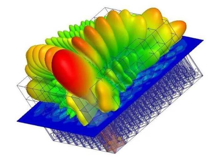
5.4. 2.4G Antenna Design Radiation Pattern
The graph indicates the directivity of radiation, that is, in which direction the radiation is greater and in which direction the radiation is smaller. This helps to accurately determine the direction of the antenna in the application.
The non-directional antenna can transmit equivalently in all directions on a plane perpendicular to the axis. But most antennas cannot achieve this ideal performance.
Each data point represents the RF field strength, which can be measured by the Receiver Signal Strength Indicator (RSSI) in the receiver. As expected, the contour image obtained is not circular because the antenna is not isotropic.
5.5. Gain of 2.4G Antenna Design
The gain provides information for comparing the radiation of the used direction with an isotropic antenna (that is, transmitting from all directions). The unit of gain is dBi, which means the radiated field strength when compared with an ideal non-directional antenna.
6. Considerations for 2.4G Antenna Design Feed
For PCB traces that feed shorter antennas, such width requirements are relatively loose. Make sure that the width of the antenna trace is the same as the width of the antenna feed contact.
7. Consideration of 2.4G Antenna Design Length
According to the different thicknesses of the PCB, the length of the MIFA antenna needs to be adjusted so that the impedance and frequency selection of the antenna radiation can be adjusted. Depending on the thickness of the circuit board, C&T RF Antennas Inc provides each antenna length.
8. The influence of environment on antenna performance
Generally, antennas used in consumer products are very sensitive to the size of the RF ground plane of the PCB and the plastic shell of the product. The antenna can be simulated as an LC resonator. When L (inductance) or C (capacitance) increases, the resonance frequency of the LC resonator will decrease. A larger RF ground plane and plastic housing will increase the effective capacitance, thereby reducing the resonance frequency.
Influence of the ground plane of 2.4G antenna design
To evaluate the sensitivity of the antenna to the size of the RF ground plane, experiments can be carried out by installing the antenna on PCBs of various possible sizes.
The larger the area of the radio frequency ground layer, the lower the resonance frequency and the better the ground layer, so the return loss will be smaller. This is the key condition in a good PCB layout.
The better the ground plane provided for the quarter-wave antenna, the better the relationship between it and the theoretical performance. This is a key concept in antenna design, which can solve the difficulty of not having enough space for grounded small modular antennas.
9. The impact of the plastic housing of 2.4G antenna design
Similarly, in order to determine the impact of the product’s plastic shell on the antenna, a wireless mouse should be used for experiments, placing the antenna in the plastic shell of the wireless mouse, and then measuring the antenna’s resonant frequency.
When the antenna is placed close to the plastic case, the resonance frequency will decrease.
The resonant frequency varies from 100MHz to 200MHz. The antenna must be re-tuned to obtain the required frequency band.
In short, increasing the size of the ground layer and the plastic casing is to reduce the resonant frequency of the antenna to the range of 100MHz to 200MHz.
Product shell and ground plane guidelines
A. It must be ensured that there are no components, fixing screws or ground planes near the tip of the antenna or the length of the antenna.
B. The battery cable or audio cable cannot pass through the same side of the antenna or the antenna wiring on the PCB.
C. Can not completely cover the antenna with the metal shell. If the product shell is metal or a protective cover, please do not completely cover the antenna.
D. The direction of the D antenna should match the direction of the final product so that the antenna has the maximum radiation in the desired direction.
E. Should have enough space: the larger the ground layer, the higher the S11 parameter value (return loss) of MIFA, IFA, chip antenna, and wire antenna.
F. There should not be any ground plane directly below the F antenna. This setting applies to all antennas.
G. There must be enough space (gap) from the antenna to the ground plane, and the width of the ground plane should be the smallest.
10. Antenna Debugging of 2.4G Antenna Design
The antenna debugging process ensures that the return loss of the antenna (viewed from the direction of the chip output) is greater than 10dB in the required frequency band. Similarly, for the chip (Balun), the same procedure must be performed to ensure that the impedance of the Balun is 50Ω in the receiving mode. At this time, both antenna debugging and Balun debugging are called antenna debugging.
The reference point is connected to a network analyzer with a port network. During antenna debugging, the connection with the chip can be disconnected by removing the Balun matching component.
During Balun debugging, the connection with the antenna matching component will be disconnected.
Simulation software helps to understand component values. However, the actual component values differ greatly from the simulated values. This happens because when the frequency is 2.4GHz, the inductance between the capacitor traces, the parasitic loading of the pad, and the ground return path create an additional parasitic loop, which completely changes the Smith chart.
For this application, you need to select a 0.7pF capacitor and a 1.2pF series capacitor to get resonance.
Use plastic and human body contact to adjust and adjust
The plastic shell of the PCB changes the antenna adjustment. All antennas are affected by near-field or far-field objects. If it is a narrowband antenna, it is very likely to be affected by near-field objects.
The plastic case and the nearby battery cable can make the antenna completely out of adjustment, and its return loss will be less than 10db in the preferred frequency band of 2.402G to 2.482G. Therefore, after debugging the empty PCB, you need to keep the PCB in the plastic shell and use the mouse to re-check and debug.
2.4G Antenna Design Summary
This 2.4G Antenna Design application note briefly introduces how to easily design the best antenna for custom products. At the same time, it also provides antenna layout guidelines for different antenna types.
C&T RF Antennas Inc not only does the 2.4G antenna design but also does the GSM antenna design, NB-IoT antenna design, 4G LTE antenna design, 5G NR antenna design, indoor-outdoor antenna design, etc.
Professional support, guidance, and advice by our RF engineers in your development process. A wide range of embedded antennas with a focus on IoT & M2M applications. Contact the CTRF team for more information.
Besides the A Complete Guide For PCB 2.4G Antenna Design article, you may also be interested in the below articles.
WiFi vs. Cellular, Is WiFi Better Than Cellular?
4G vs. 5G: What is the difference between 4G and 5G?
How to Choose the Best Antenna for Lora?