This article describes the 1dB gain compression point overview and testing.
Semiconductor devices are very bright stars in the modern electronics industry, in recent decades has been a great development, with many advantages, have been widely used in control, conversion, amplification, arithmetic, and other functional circuits, and have been much favored.
Love should accept its shortcomings, everything has its own shortcomings, and semiconductor devices are no exception. For active devices such as RF amplifiers covered in this paper, nonlinearity is one of its drawbacks.
Nonlinearity is a topic that PA, LNA, and other RF active devices can not get around, although it is unavoidable, still want to try to keep it at a relatively low level to reduce the impact on the system.
There are more parameters to measure the nonlinear characteristics, of which a 1dB gain compression point is usually a must-measure item.
How nonlinearity is generated, why it causes gain compression, and how to test the 1dB gain compression point will be the focus of the following section.
How is nonlinearity generated?
One of the reasons why semiconductor devices are widely used is that they can be “controlled” and used by people. For a basic transistor, for example, a field-effect tube, the on/off of the transistor can be controlled by controlling the power supply to the gate, and the amount of current between the drains can be controlled.
Transistors can be used to design RF amplifiers where the slope of the transistor transfer characteristic curve (transconductance) determines the gain of the amplifier to some extent. However, the transfer characteristic curve of a transistor is not linear, which means that the gain of the amplifier is not constant either.
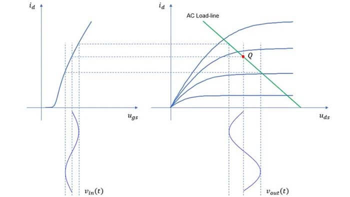
Figure 1. Transistor DC characteristic curve and signal amplification diagram
In the case of a common-source amplifier, for example, the gate is used as the AC signal input port, and the amplified signal is output from the drain. When the DC operating point Q is designed, the RF signal is superimposed on the operating point voltage of the gate, and then amplified and output.
Figure 1 gives a typical transfer and output characteristic curve of the transistor and a schematic diagram of the process by which the AC signal is amplified.
When the RF input signal is relatively small, the region mapped onto the transfer characteristic curve is close to linear and the signal can be approximated as being linearly amplified if the DC operating point is properly selected.
As the power of the RF signal increases, the area mapped to the transfer characteristic curve gradually becomes nonlinear, and the amplified waveform is significantly different from the input signal at this time, and the distortion becomes more and more obvious.
This distortion is not a linear distortion of the overall amplification or reduction of the waveform, but a nonlinear distortion.
Taking Figure 1 as an example, consider an extreme case: assuming that a DC operating point has been selected when the input signal increases to the point that the gate-source voltage Vgs is below the conduction threshold voltage at some moments, the transistor will turn off at these moments, and of course, there will be no output waveform, so the output waveform will be severely distorted, which also means that the amplifier is already in a severe nonlinear operating state!
If the DC operating point is chosen properly, the amplifier may operate over a wide range of input powers without significant non-linear distortion.
And if it is not chosen properly, such as near the conduction threshold voltage, then even if the input signal is small, there may be significant nonlinear distortion.
Having said that, the main factors affecting the linearity of the amplifier include the transfer characteristics of the nonlinearity, the choice of the DC operating point, and the strength of the input signal.
The mechanism of nonlinear distortion in semiconductor devices may be far more complex than the above introduction, but the three factors mentioned above are at least partially responsible for it.
Nonlinear characteristics are indeed detrimental for amplifiers, but some devices are meant to use such characteristics to achieve specific functions, such as multipliers, mixers, frequency multipliers, etc. The key depends on the specific application.
What is the 1dB gain compression point?
The output signal of a nonlinear circuit can usually be expanded on a Taylor level, or more specifically, on a Maclaurin level.
Where vin(t) and vout(t) are the input and output signals, respectively, and ci is the constant coefficient of the level expansion.
What is the output characteristic of the amplifier when fed with a single frequency point signal?
Let vin (t) = V0 cosω0 t, and substitute it into the above equation to obtain
The components of the above equation can be expanded as follow
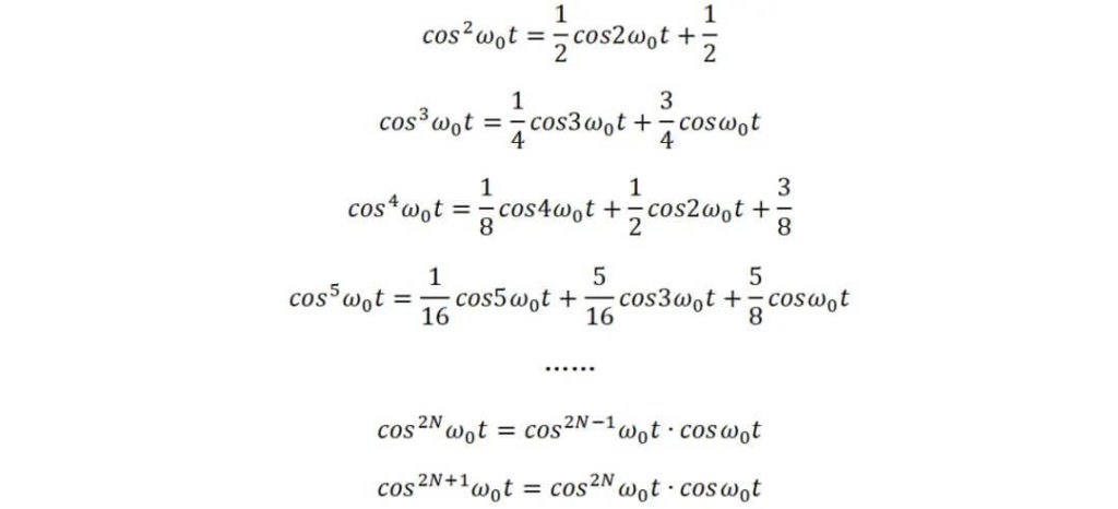
(a) For even powers, the DC component and the even harmonic component are the only components after the summation, which can be abbreviated as 2i-ꞷ0, I being a non-negative integer.
For odd powers, only the odd harmonic component (2i+1)-ꞷ0, i is a non-negative integer, after the summation and difference.
It can be seen that, due to the nonlinear characteristics of the amplifier, when a single frequency point signal is input, its output signal will regenerate some new frequency components in addition to the original frequency point signal that is amplified, and frequency regeneration also becomes a characteristic of nonlinear distortion.
For the frequency component ꞷ0, the output term is
Taylor level expansion, the higher the order, the smaller the constant-coefficient ci, therefore, for convenience, only the first three terms are considered in the above equation, ignoring the higher terms.
Then the voltage gain of the amplifier is

The gain can be divided into two parts: the linear amplification gain and the gain contributed by the influence of the input signal.
G=c1+∆G(V0)
Theoretically, the amplifier is expected to be ideally linear, with the output power increasing linearly regardless of the input power, i.e., the gain is constant.
However, the fact is that when the input power is large, the amplifier enters the nonlinear operating region, resulting in gain compression. Therefore, ∆G(V0 ) in the above equation is less than 0.
When the input power is low, the gain part associated with the input signal tends to 0, then the gain at this point is close to the linear gain.
As the input power increases, the output power increases approximately linearly, to a certain extent, the nonlinearity becomes more and more obvious, leading to gain compression, and the output power growth slows down, and finally gradually tends to saturation and stability, the relationship between input and output power is shown in Figure 2.
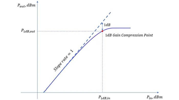
Figure 2: Gain compression characteristics of the amplifier and 1dB gain compression point
How to interpret the curve relationship in Figure 2?
First of all, it should be clear that this is a logarithmic representation of the input and output power, so the slope of the curve for an ideal linear amplifier is 1, as shown by the dotted line in the figure.
The solid line characterizes the relationship between the actual input and output power of the amplifier. As the input power increases, the output power increases at a slower rate, deviating more and more from the ideal curve, and the gain gradually becomes lower, which is the gain compression effect.
Pout (dBm)=Pin ( dBm)+G(dB)
Amplifiers and other active devices are usually concerned about the actual gain than the linear gain drop of 1dB, called the 1dB gain compression point, the point corresponds to the input and output power is generally marked as P1dB, in and P1dB, out respectively.
The higher the 1dB gain compression point is, the better. When comparing two amplifiers, the higher the compression point is, the better the linearity is.
In a wireless communication system, the signal usually has a certain bandwidth, if the total power is close to the 1dB compression point, the more the amplifier nonlinearity tends to be obvious, it will produce stronger harmonics, and cross-tuning products, thus causing interference to the neighboring band or in-band.
Therefore, nonlinear distortion is a very important consideration in amplifier design.
How to test the 1dB gain compression point?
The previous section briefly introduced the basic content of gain compression due to nonlinearity, then how to test the 1dB gain compression point in practice?
1dB gain compression point test method is more flexible, through the vector network analyzer automatic test, you can automatically test the compression point when the 1D / 2D scan; can also be based on the signal source and spectrum meter or even power meter for manual testing, which will be the following to highlight the method.
Signal source output power and the set value of a certain deviation, and the test required cable, attenuator, and other accessories have a certain loss, then the need for this early calibration?
As the P1dB test is the absolute power, so the above factors still affect the test results. However, there is no need for a full calibration.
The P1dB test idea introduced below is to first determine the signal source output power setting how much gain compression 1dB, and then record the set power and the power measured by the spectrum meter, and finally deduct the loss of the cable and accessories to determine the input and output power and gain of the 1dB compression point, respectively.
It is worth mentioning that the test requires good linearity of the output power of the signal source, otherwise, it will bring a large test error.
The good thing is that the general-purpose RF source has good linearity in a wide power range. Of course, in order to further improve the test accuracy, you can also consider using a power meter to signal source in a certain power range for power calibration to further improve the output power linearity.
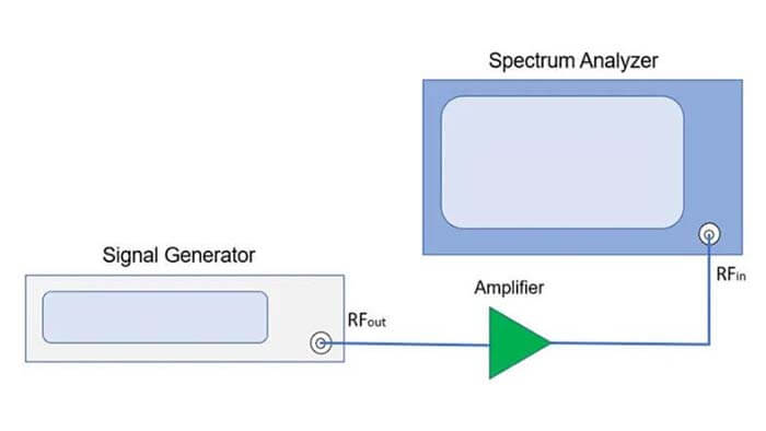
Figure 3. Typical connection schematic for 1dB gain compression point test
For the actual test, the specific operation steps are as follows.
(1) 1dB gain pre-test preparation.
Select good-performance RF cables, adapters, and suitable high-power capacity attenuators, for cables and adapters, especially to ensure that the VSWR in the test band is good.
The high-power capacity attenuator is only needed when testing PA to protect the test equipment, for small signal amplifier testing, the use of the spectrum meter built-in attenuator is sufficient.
(2) 1dB gain test connection.
In accordance with Figure 3 to complete the test connection, if the test PA, it is necessary to introduce a suitable attenuator after, at this time to ensure that the signal source does not have RF signal output.
(3) 1dB gain amplifier parameter settings.
Set the frequency, power, and power step of the signal source, the frequency is set according to the test frequency, it is recommended to set a low power first to ensure that the amplifier works in the approximately linear region.
Set the center frequency CF and Span of the spectrometer, because the test single frequency point signal, it is recommended that Span is not too large, and the setting of internal attenuation needs to be considered according to the input power, gain, and external attenuation of the amplifier.
(4) Turn on the amplifier.
Pay attention to the power-on sequence, especially for PA, see the notes below for details. It is recommended to power up the gate first and then the drain.
(5) P1dB gain test.
Turn on the output switch of the signal source, adjust the reference level and attenuation of the spectrum meter, so that the CW signal spectrum is well displayed, and ensure sufficient signal-to-noise ratio. Call out the spectrum meter’s peak marker, and record the power of the signal source setting Pin,1 and the power of the peak marker Pout,1.
The power output of the signal source can be increased continuously by using the navigation keys of the signal source to gradually increase the power according to the step set in step (2) and observe the power measured by the spectrum meter. When the power of the signal source is adjusted to Pin,n, and the following equation is satisfied
Pin,n-Pin,1-(Pout,n-Pout,1)=1dB gain
Then the first step of the P1dB gain test is completed, but Pin,n, and Pout,n is not yet 1dB gain compression point input and output power.
Pout,n is the measured power of the amplifier output power after passing through the rear cables, attenuators, and other accessories, so after compensating for these losses, we get P1dB, out.
Pin,n is the amplifier gain compression 1dB when the power of the signal source settings, remove the amplifier, the direct use of spectrum test amplifier input side of the power that is P1dB, in. 1dB compression point corresponding to the amplifier gain is
G1dB=P1dB,out-P1dB,in
What do I need to pay attention to in the P1dB gain test?
First of all, the amplifier power-up sequence should be correct, especially for power amplifiers. For GaAs and GaN amplifiers, most of them are designed with depletion transistors, and the gate-source voltage is 0V when it is open, so the gate of these amplifiers generally works in negative voltage. For this type of amplifier, for protection purposes, negative gate voltage must be added first, and then drain voltage.
Second, when testing the PA, it is necessary to select the appropriate attenuator according to its maximum output power, so as not to burn out the RF front-end of the spectrum meter with too much power. The internal attenuator of the spectrum meter can usually only withstand a maximum of 1W of power, so the power after the external attenuator must be much less than that value.
Finally, considering the test accuracy, a suitable attenuator can be introduced before and after the amplifier to improve the input and output matching. For PA testing, due to certain requirements on the driving power, the attenuation before the PA should not be too large, to ensure that the power of the signal source after this attenuator can still drive the PA to work properly.
In addition, to avoid the spectrum meter in the non-linear region, you can refer to the specifications of the spectrum meter to find its P1dB gain, as long as the power fed into the spectrum meter during the test is at least 6dB below the value, then the impact of the spectrum meter’s own non-linearity can be ignored.
There is a simple method of judgment when the 1dB gain compression point is found, which manually increases the attenuation of the spectrum meter, if the measured signal power remains basically unchanged, then the spectrum meter does not have obvious nonlinearity.
If the measured power becomes larger instead of increasing the attenuation, it means that the RF front-end of the spectrum meter has been compressed, and it is necessary to further increase the attenuation until the measured power is stable, and then continue to increase the output power of the signal source to find the real 1dB gain compression point of the amplifier.
Finally, leave an open question.
For PA, there may be a situation where the gain does not always show a monotonically decreasing trend when the excitation power is increasing, for example, as the excitation power increases, the PA gain may first increase and then decrease, so when calibrating the 1dB gain compression point, which gains (or power) should be used as a reference?
Besides this What is A 1dB gain Compression Point article, you may also be interested in the below articles.
What is the difference between WIFI and WLAN?
Summary of 41 Basic Knowledge of LTE
What Is The 5G Network Slicing?