Description
What is RF Power Amplifier 2.4 GHz Amplifier?
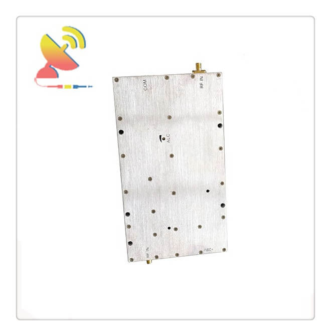
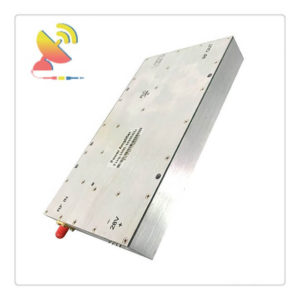
The RF Power Amplifier 2.4 GHz CTRF-ANTENNA-AMP-PA-2450-60W 2.4GHz Amplifier 60 Watt RF Power Amplifier is a power amplifier with 2400-2500Mhz wifi frequency and a 60-watt power amplifier supplied by C&T RF Antennas Inc.
RF Power Amplifier 2.4 GHz Amplifier is supplied by C&T RF Antennas Inc, we provide RF products with RF antennas, Antenna Accessories, Amplifiers, And Repeaters.
C&T RF Antennas Inc provides internal & external antennas with antenna radio frequencies such as NFC, 169MHz, 230MHz, 315MHz, 433MHz, 868MHz, 915MHz, VHF&UHF, Lora, NB-IoT, ADS-B, GSM, GNSS, GPRS, 1.2 GHz, 1.4 GHz, 1.8 GHz, Wi-Fi 2.4 GHz, 5.8 GHz, Cellular 2G, 3G, 3.5 GHz, 4G LTE, GPS, 5G NR, 6G, etc.
C&T RF Antennas Inc. provides RF antennae with Omni & Directional antenna types such as Dipole Antennas, Whip Antennas, Marine Antennas, Router Antennas, MIMO Antennas, Combo Antennas, PCB Antennas, FPC Antennas, Spring Antennas, Magnetic Antennas, Sector Antennas, Yagi Antennas, and Accessories, etc, for IoT & M2M industries.
RF Power Amplifier 2.4 GHz 60 Watt RF Power Amplifier Is Available At C&T RF Antennas Inc. We offer the RF Power Amplifier 2.4 GHz Inventory, RF Power Amplifier 2.4 GHz Pricing, & RF Power Amplifier 2.4 GHz Datasheets.
If you cannot find the one that you are looking for, please contact our C&T RF sales team for support, thank you.
RF Power Amplifier 2.4 GHz Technical Specifications:
| Model | CTRF-ANTENNA-AMP-PA-2450-60W |
| Frequency(MHz) | 2400-2500 |
| Input Power | ≤20dBm |
| Output Power(W) | 48±1(50W ) |
| ALC Range(dB) | ≥25 |
| In-Band ripple(dB) | ±3 |
| Gain(dB) | 55 or Customized |
| Gain Adjustment Range(dB) | >31/1dB step or Customized |
| Gain Adjustment Linearity(dB) | ≤±1 |
| Gain Flatness(dB) | ±0.5(Max) |
| Impedance(ohm) | 50 |
| VSWR | ≤1.4:1 |
| Voltage(V) | DC+28 |
| Power Current | ≤11A |
| RF Connector | SMA-50K or other Customized |
| Monitor interface | RS-485 or RS232 or other Customized |
| Monitoring communication protocols | Use the Manufacturer’s protocol or Customized |
| Working Temperature | -40~+65 degree |
| Storage Temperature | -55 to +85 degree |
| Operating Humidity | 0 to 90%, relative |
| Surface Color | Metal color conductive oxide and other color customized |
| weight | ≤1.0Kg |
| Remark | Module with output short circuit or open circuit protection |
RF Power Amplifier 2.4 GHz Monitoring Function Description:
| No. | Monitoring function | Description | |
| 1 | query | PA ALARM | When an alarm amplifier failure |
| 2 | SWR ALARM | Amplifier output reflection is too large, VSWR exceeds3:1, an alarm is generated | |
| 3 | Over-temperature alarm | Module internal temperature exceeds85 ℃ generates an alarm and turns off the amplifier until the temperature returns tobelow65 ℃,re-open the amplifier | |
| 4 | Over-output power alarm | When the output power exceeds the nominal full power 2dB is an alarm | |
| 5 | Input power detection | Accuracy of± 1dB | |
| 6 | Reverse power detection | Accuracy of± 1dB | |
| 7 | Output power detection | Detecting the actual output power amplifier, Accuracy of± 1dB | |
| 8 | Temperature detection | Detection module operating temperature, detection range: -25 ~ +90 ℃, Accuracy of± 3 ℃ | |
| 10 | SWR | Detecting amplifier output port VSWR range of 1.2~ 4.0 | |
| 11 | query and set | PA attenuator Set and query | Set and query the value of ATT |
| 12 | PA switching query and set | Query and set the state open tube amplifier | |
Choice of op-amp structure
There are three important operational amplifier structures: (a) simple two-stage op-amp, (b) folded cascade, (c) cascade.
The design index of the operational amplifier designed this time requires a differential output amplitude of ±4V, that is, the sum of VDSAT and N of all NMOS transistors at the output end is less than 0.5V, and the sum of VDSAT and P of all PMOS transistors at the output end must also be less than 0.5V.
Main op amp structure
The operational amplifier has two stages:
(1) Cascode stage increases DC gain (M1-M8);
(2) Common source amplifier (M9-M12).
Common mode negative feedback
For a fully differential op-amp, in order to stabilize the output common-mode voltage, a common-mode negative feedback circuit should be added.
When designing a fully differential operational amplifier with balanced output, the following points must be considered:
The open-loop DC gain of common-mode negative feedback is required to be large enough, and it is best to be equivalent to the differential open-loop DC gain;
The unity-gain bandwidth of common-mode negative feedback is also required to be large enough, preferably close to the differential unity-gain bandwidth;
In order to ensure the stability of common-mode negative feedback, common-mode loop compensation is generally required;
Common-mode signal monitors are required to have good linearity characteristics; common-mode negative feedback has nothing to do with differential-mode signals, even if the differential-mode signal path is turned off.
The operational amplifier adopts a continuous-time model to realize the common-mode negative feedback function.
This structure shares the current mirror and output load in the input stage of the common-mode amplifier and the differential-mode amplifier. In this way, power consumption is reduced on the one hand;
On the other hand, it is ensured that the common-mode amplifier and the differential-mode amplifier maintain the same AC characteristics.
Because the output stage of the common-mode amplifier and the output stage of the differential-mode amplifier can be completely shared, the capacitance compensation circuit is the same.
As long as the frequency characteristic of the differential mode amplifier is stable, the common mode of negative feedback is also stable.
This common-mode negative feedback circuit allows the fully differential operational amplifier to be designed like a single-ended output operational amplifier, regardless of the effect of the common-mode negative feedback circuit on the fully differential amplifier.
Voltage bias circuit: wide swing current
Three voltage biases are required in the cascade input stage. In order to make the dynamic range of the input stage larger, a wide swing current source is used to generate the required three bias voltages.
Reviews
There are no reviews yet.