What is PCB (Printed Circuit Board)?
A printed circuit board (PCB) mechanically supports and electrically connects electrical or electronic components using conductive tracks, pads, and other features etched from one or more sheet layers of copper laminated onto and/or between sheet layers of a non-conductive substrate.
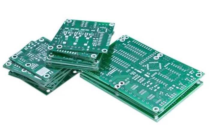
PCB (Printed Circuit Board) is important electronic component support for electronics and a carrier for the electrical interconnection of electronic components. Because it is made by electronic printing, it is called a printed circuit board.
PCB (printed circuit board) is one of the important parts of the electronics industry. Almost every kind of electronic equipment, from electronic watches, and calculators, to computers, communication electronic equipment, and military weapon systems, as long as there are electronic components such as integrated circuits, order make the electrical interconnection between the various components must be printed.
The PCB's function
After electronic equipment adopts printed boards, due to the consistency of similar printed boards, manual wiring errors can be avoided, and electronic components can be automatically inserted or mounted, automatic soldering, and automatic detection, ensuring the quality of electronic equipment, Improve labor productivity, reduce costs, and facilitate maintenance.
The printed circuit board is composed of an insulating bottom plate, connecting wires, and pads for assembling and welding electronic components, and has the dual functions of conductive lines and insulating bottom plates.
It can replace complex wiring and realize the electrical connection between the various components in the circuit, which not only simplifies the assembly and welding of electronic products, but also reduces the workload of wiring in the traditional way, and greatly reduces the labor intensity of workers;
Moreover, the volume of the whole machine is reduced, the cost of the product is reduced, and the quality and reliability of electronic equipment are improved. The printed circuit board has good product consistency, and it can adopt a standardized design, which is conducive to the realization of mechanization and automation in the production process.
At the same time, the entire printed circuit board that has been assembled and debugged can be used as an independent spare part to facilitate the interchange and maintenance of the entire product. At present, printed circuit boards have been extremely widely used in the manufacturing of electronic products.
The earliest printed circuit boards used paper-based copper-clad printed boards. Since the emergence of semiconductor transistors in the 1950s, the demand for printed boards has risen sharply. In particular, the rapid development and wide application of integrated circuits have made the volume of electronic equipment smaller and smaller, and the density and difficulty of circuit wiring have become greater and greater, which requires continuous updating of printed boards.
At present, the variety of printed boards has developed from single-sided boards to double-sided boards, multilayer boards, and flexible boards;
The structure and quality have also been developed to ultra-high density, miniaturization, and high reliability.
New design methods, design supplies, board-making materials, and board-making techniques continue to emerge.
In recent years, various computer-aided design (CAD) printed circuit board application software has been popularized and promoted in the industry. Among specialized printed board manufacturers, mechanized and automated production has completely replaced manual operations.
PCB Board Features
The reason why PCB can be more and more widely used is that it has many unique advantages, roughly as follows.
Can be high-density
The high density of printed boards has been able to develop correspondingly with the improvement of integrated circuit integration and the advancement of mounting technology.
High reliability
Through a series of inspections, tests and aging tests, and other technical means, the PCB can be guaranteed to work reliably for a long time (usually 20 years).
Designability
The requirements for various properties of PCB (electrical, physical, chemical, mechanical, etc.) can be achieved through design standardization and standardization. In this way, the design time is short and the efficiency is high.
Manufacturability
PCB board adopts modern management, which can realize standardization, scale (quantity), and automatic production, so as to ensure the consistency of product quality.
Testability
PCB products are not only convenient for standardized assembly of various components, but also for automated and large-scale mass production. In addition, by assembling the PCB and various other components as a whole, larger parts and systems can be formed to the complete machine.
Maintainability
Since PCB products and various components are assembled in a standardized design and large-scale production, these components are also standardized. Therefore, once the system fails, it can be replaced quickly, conveniently, and flexibly, and the system can be quickly restored to work.
PCB has other advantages, such as miniaturization and lightweight of the system, and high-speed signal transmission.
PCB has the following functions in electronic equipment.
(1) Provide mechanical support for the fixing and assembly of various electronic components such as integrated circuits, realize the wiring and electrical connection or electrical insulation between various electronic components such as integrated circuits, and provide the required electrical characteristics.
(2) Provide solder mask graphics for automatic welding, and provide identification characters and graphics for component insertion, inspection, and maintenance.
(3) After electronic equipment adopts printed boards, due to the consistency of similar printed boards, manual wiring errors can be avoided, and electronic components can be automatically inserted or mounted, automatic soldering, and automatic detection, ensuring electronic products The quality of the product improves labor productivity, reduces costs, and facilitates maintenance.
(4) Provide required electrical characteristics, characteristic impedance, and electromagnetic compatibility characteristics for circuits in high-speed or high-frequency circuits.
(5) The printed circuit board with passive components embedded inside provides certain electrical functions, simplifies the electronic installation procedure, and improves the reliability of the product.
(6) In large-scale and ultra-large-scale electronic packaging components, an effective chip carrier is provided for the miniaturized chip packaging of electronic components.
Classified by layer
Classification according to the number of circuit layers: divided into single-sided, double-sided and multi-layer boards. Common multi-layer boards are generally 4-layer boards or 6-layer boards, and complex multi-layer boards can reach dozens of layers. The PCB board has the following three main types of division.
Single-Sided PCB Boards
On the most basic PCB, the parts are concentrated on one side, and the wires are concentrated on the other side (when there are SMD components and the wires are on the same side, the plug-in device is on the other side). Because the wires only appear on one side, this kind of PCB is called a single-sided (Single-sided).
The single-sided boards have many strict restrictions on the design of the circuit (because there is only one side, the wiring cannot cross and must be around a separate path), so only early circuits use this type of board.
Double-Sided PCB Boards
This kind of circuit board has wiring on both sides, but to use wires on both sides, there must be a proper circuit connection between the two sides. The connection bridge between such circuits is called a via. A via is a small hole filled or coated with metal on the PCB, which can be connected with the wires on both sides.
Because the area of the double-sided board is twice as large as that of the single-sided board, the double-sided board solves the difficulty of interlacing wiring in the single-sided board (it can be conducted to the other side through holes), and it is more suitable for use in circuits that are more complicated than the single-sided board.
Multi-Layer PCB Boards
In order to increase the area that can be wired, multi-layer boards use more single or double-sided wiring boards. Use one double-sided as the inner layer, two single-sided as the outer layer, two double-sided as the inner layer, and two single-sided as the outer layer of the printed circuit board.
The positioning system and the insulating bonding material alternately together and the conductive pattern Printed circuit boards that are interconnected according to design requirements become four-layer and six-layer printed circuit boards, also known as multilayer printed circuit boards.
The number of layers of the board does not mean that there are several independent wiring layers. In special cases, empty layers are added to control the thickness of the board. Usually, the number of layers is even and includes the two outermost layers. Most of the motherboards have 4 to 8 layers of structure, but technically, it is possible to achieve nearly 100 layers of PCB boards.
Most large supercomputers use fairly multi-layered motherboards, but because these types of computers can already be replaced by clusters of many ordinary computers, super-multilayered boards have gradually ceased to be used. Because the various layers in the PCB are tightly integrated, it is generally not easy to see the actual number, but if you look closely at the motherboard, you can still see it.
Classified by soft and hard
Divided into rigid circuit boards and flexible circuit boards, flexible and rigid boards. Generally, the PCB shown in the first picture below is called a rigid (Rigid) PCB, and the yellow connecting line in the second picture is called a flexible (or turbulent Flexible) PCB or FPC board.
The intuitive difference between rigid PCB and flexible PCB is that flexible PCB can be bent. The common thickness of rigid PCB is 0.2mm, 0.4mm, 0.6mm, 0.8mm, 1.0mm, 1.2mm, 1.6mm, 2.0mm, etc. The common thickness of flexible PCB is 0.2mm, and the parts to be welded will have a thick layer behind them. The thickness of the thick layer varies from 0.2mm to 0.4mm.
The purpose of understanding these is to provide structural engineers with a spatial reference when designing. Common materials for rigid PCB include phenolic paper laminate, epoxy paper laminate, polyester glass mat laminate, and epoxy glass cloth laminate.
Common materials for flexible PCB include polyester film, polyimide film, and fluorinated ethylene propylene film.
PCB board design principles
To get the best performance of the electronic circuit, the layout of the components and the layout of the wires are very important. In order to design PCB with good quality and low cost. The following general principles should be followed.
Layout
First, consider the PCB size. The PCB size is too large, the printed lines are long, the impedance increases, the anti-noise ability is reduced, and the cost also increases; if the PCB size is too small, the heat dissipation will not be good, and the adjacent lines easily interfere. After determining the PCB size, determine the location of the special components. Finally, according to the functional units of the circuit, all the components of the circuit are laid out.
Observe the following principles when determining the location of special components.
① Shorten the wiring between high-frequency components as much as possible, and try to reduce their distribution parameters and mutual electromagnetic interference. Components that are susceptible to interference should not be too close to each other, and input and output components should be as far away as possible.
② There may be a high potential difference between some components or wires. The distance between them should be increased to avoid accidental short circuits caused by the discharge. The components with high voltage should be arranged as far as possible in places that are not easily reachable by hand during debugging.
③ Components weighing more than 15 g should be fixed with brackets and then welded. Those components that are large, heavy, and generate a lot of heat should not be installed on the printed circuit board but should be installed on the chassis bottom plate of the whole machine, and the heat dissipation problem should be considered. Thermal components should be far away from heating components.
④ The layout of adjustable components such as potentiometers, adjustable inductance coils, variable capacitors, micro switches, etc. should consider the structural requirements of the whole machine. If it is adjusted inside the machine, it should be placed on the printed circuit board where it is convenient for adjustment; if it is adjusted outside the machine, its position should match the position of the adjustment knob on the chassis panel.
According to the functional unit of the circuit, when laying out all the components of the circuit, the following principles must be met.
① Arrange the position of each functional circuit unit according to the circuit flow so that the layout is convenient for signal circulation, and the signal is kept in the same direction as possible.
② Take the core component of each functional circuit as the center and layout around it. The components should be pulled uniformly, neatly, and compactly on the PCB to minimize and shorten the leads and connections between the components.
③ For circuits operating at high frequencies, the distributed parameters between components must be considered. Generally, the circuit should be arranged in parallel as much as possible. In this way, it is not only beautiful, but also easy to install and weld, and easy to mass-produce.
④ The components located at the edge of the circuit board are generally not less than 2 mm away from the edge of the circuit board. The best shape of the circuit board is rectangular. The aspect ratio is 3:2 or 4:3. When the size of the circuit board is larger than 200 mmx150 mm, the mechanical strength of the circuit board should be considered.
Wiring
The principle is as follows.
① The wires used for the input and output terminals should try to avoid being adjacent and parallel. It is best to add ground wires between wires to avoid feedback coupling.
② The minimum width of the conductors of the printed circuit board is mainly determined by the adhesion strength between the conductors and the insulating substrate and the current value flowing through them.
When the thickness of the copper foil is 0.05 mm and the width is 1 to 15 mm, the temperature will not be higher than 3°C through a current of 2 A, so a wire width of 1.5 mm can meet the requirements. For integrated circuits, especially digital circuits, a wire width of 0.02 to 0.3 mm is usually selected. Of course, as long as possible, use as wide a line as possible, especially the power line and the ground line.
The minimum spacing of wires is mainly determined by the worst-case insulation resistance and breakdown voltage between the wires. For integrated circuits, especially digital circuits, as long as the process permits, the pitch can be as small as 5 to 8 um.
③ The bends of the printed conductors are generally arc-shaped, and the right angle or angle will affect the electrical performance in the high-frequency circuit. In addition, try to avoid the use of large-area copper foil, otherwise, the copper foil will easily expand and fall off when heated for a long time. When a large-area copper foil is required, it is best to use a grid shape, which helps to eliminate the volatile gas generated by the adhesive between the copper foil and the substrate.
Pad
The center hole of the pad is slightly larger than the diameter of the device lead. If the pad is too large, it is easy to form a false solder. The outer diameter D of the pad is generally not less than d+1.2 mm, where d is the lead diameter. For high-density digital circuits, the minimum diameter of the pad can be d+1.0 mm.
PCB Industry
Classified according to the upstream and downstream of the industry chain, it can be divided into raw materials, copper-clad laminates, printed circuit boards, electronic product applications, etc. The relationship is as simple as the following.
Fiberglass cloth
Fiberglass cloth is one of the raw materials for copper-clad laminates, which are woven from fiberglass yarns, which account for about 40% (thick board) or 25% (thin board) of the cost of copper-clad laminates.
The glass fiber yarn is calcined into a liquid state from raw materials such as silica sand in a kiln. It is drawn into a very fine glass fiber through a very small alloy nozzle, and then hundreds of glass fibers are twisted into a glass fiber yarn. The construction investment of the kiln is huge, usually hundreds of millions of funds, and once it is ignited, it must be produced 24 hours a day, and the cost of entry and exit is huge.
Copper foil
Copper foil is the raw material that accounts for the largest proportion of the cost of copper-clad laminates, accounting for about 30% (thick plate) or 50% (thin plate) of the cost of copper-clad laminates. Therefore, the price increase of copper is the main driving force for the price increase of copper-clad laminates.
Copper Clad Laminate
Copper-clad laminate is a product made by pressing glass fiber cloth and copper foil together as a fusion agent with epoxy resin, etc. It is the direct raw material of printed circuit boards and is made into printed circuits after etching, electroplating, and multi-layer board pressing.
C&T RF Antennas Inc supplies the PCB antenna design, FPC antenna design, and internal & external product manufacturing, contact the C&T RF engineering team for more information.
Besides the PCB (Printed Circuit Board) article, you may also be interested in the below articles.
What is the difference between WIFI and WLAN?
Summary of 41 Basic Knowledge of LTE
What Is The 5G Network Slicing?