The heat generated when the electronic equipment is working causes the internal temperature of the equipment to rise rapidly.
If the heat is not dissipated in time, the equipment will continue to heat up, the device will fail due to overheating, and the reliability of the electronic equipment will decrease.
Therefore, it is very important to dissipate heat from the circuit board. We will show you the 11 PCB Heat Dissipation Techniques in this article.
Analysis of Temperature Rise of Printed Circuit Board
The direct cause of the temperature rise of the printed circuit board is the existence of circuit power consumption devices. Electronic devices all have power consumption to varying degrees, and the heating intensity varies with the size of the power consumption.
Two phenomena of temperature rise in printed circuit boards
(1) Local temperature rise or large area temperature rise;
(2) Short-term temperature rise or long-term temperature rise.
When analyzing PCB thermal power consumption, it is generally analyzed from the following aspects.
Electrical power consumption
(1) Analyze the power consumption per unit area;
(2) Analyze the distribution of power consumption on the PCB circuit board.
The structure of the printed circuit board
(1) The size of the printed circuit board;
(2) The material of the printed circuit board.
How to install the printed circuit board
(1) Installation method (such as vertical installation, horizontal installation);
(2) The sealing condition and the distance from the casing.
Heat radiation
(1) The emissivity of the printed circuit board surface;
(2) The temperature difference between the printed circuit board and the adjacent surface and their absolute temperature;
Heat Conduction
(1) Install the radiator;
(2) Conduction of other installation structures.
Heat convection
(1) Natural convection;
(2) Forced cooling convection.
The analysis of the above factors from the PCB trace board is an effective way to solve the temperature rise of the printed board. Often these factors in a product and system are interrelated and dependent. Most of the factors should be analyzed according to the actual situation.
The specific actual situation can calculate or estimate the parameters such as temperature rise and power consumption more correctly.
11 kinds of PCB Heat Dissipation Techniques
The heat dissipation of the PCB circuit board is a very important link, so what are the techniques for the heat dissipation of the PCB circuit board?
PCB Heat Dissipation Techniques 1
Heat dissipation through the PCB board itself
At present, the widely used PCB boards are copper-clad/epoxy glass cloth substrates or phenolic resin glass cloth substrates, and a small amount of paper-based copper-clad boards are used.
Although these substrates have excellent electrical properties and processing properties, they have poor heat dissipation. As a heat dissipation path for high-heating components, it is almost impossible to expect heat from the resin of the PCB itself to conduct heat, but to dissipate heat from the surface of the component to the surrounding air.
However, as electronic products have entered the era of miniaturization of components, high-density mounting, and high-heating assembly, it is not enough to rely on the surface of a component with a very small surface area to dissipate heat.
At the same time, due to the extensive use of surface mount components such as QFP and BGA, a large amount of heat generated by the components is transferred to the PCB board.
Therefore, the best way to solve the problem of heat dissipation is to improve the heat dissipation capacity of the PCB itself, which is in direct contact with the heating element, through the PCB board conducted or radiated.
PCB plus heat dissipation copper foil and copper foil with large area power supply
PCB thermal vias
Exposure of copper on the back of the IC reduces the thermal resistance between the copper skin and the air
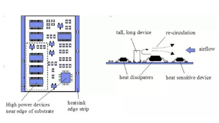
Heat-sensitive components are placed in the cold wind area.
The temperature detection device is placed in the hottest position.
The devices on the same printed board should be arranged as far as possible according to their calorific value and degree of heat dissipation. Devices with low calorific value or poor heat resistance (such as small-signal transistors, small-scale integrated circuits, electrolytic capacitors, etc.) should be placed in cooling at the top of the airflow (at the entrance), devices with large heat or heat resistance (such as power transistors, large-scale integrated circuits, etc.) are placed at the most downstream of the cooling airflow.
In the horizontal direction, the high-power devices are arranged as close to the edge of the printed board as possible to shorten the heat transfer path; in the vertical direction, the high-power devices are arranged as close as possible to the top of the printed board to reduce the influence of these devices on the temperature of other devices.
The heat dissipation of the printed board in the equipment mainly relies on airflow, so the airflow path should be studied during the design, and the device or printed circuit board should be reasonably configured.
When air flows, it always tends to flow in places with low resistance, so when configuring devices on a printed circuit board, avoid leaving large airspace in a certain area. The configuration of multiple printed circuit boards in the whole machine should also pay attention to the same problem.
The temperature-sensitive device is best placed in the lowest temperature area (such as the bottom of the device). Never place it directly above the heating device. It is best to stagger multiple devices on the horizontal plane.
Place the devices with the highest power consumption and heat generation near the best position for heat dissipation. Do not place high-heating devices on the corners and peripheral edges of the printed board, unless a heat sink is arranged near it.
When designing the power resistor, choose a larger device as possible, and make it have enough space for heat dissipation when adjusting the layout of the printed board.
PCB component spacing suggestions as the below shows.
PCB Heat Dissipation Techniques 2
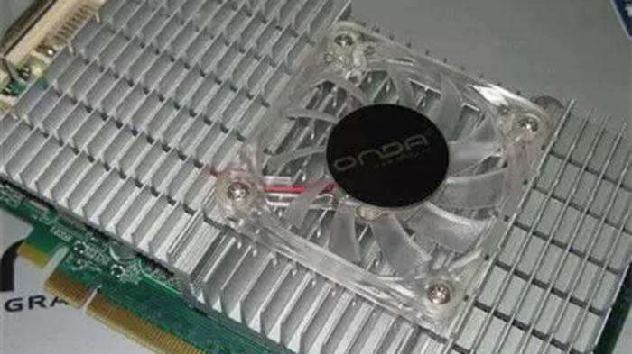
Among high-heating components plus radiators and heat-conducting plates, when a few PCB components generate a large amount of heat (less than 3), a heat sink or heat pipe can be added to the heat-generating components. When the temperature cannot be lowered, use a radiator with a fan to enhance the heat dissipation effect.
When the number of heating devices is large (more than 3), a large heat dissipation cover (board) can be used, which is a special heat sink customized according to the position and height of the heating device on the PCB or a large flat heat sink Cut out different component height positions. The heat dissipation cover is integrally buckled on the surface of the component, and it contacts each component to dissipate heat.
However, the heat dissipation effect is not good due to the poor consistency of height during the assembly and welding of components. Usually, a soft thermal phase-change thermal pad is added to the surface of the component to improve the heat dissipation effect.
PCB Heat Dissipation Techniques 3
For equipment that adopts free convection air cooling, it is best to arrange integrated circuits (or other devices) vertically or horizontally.
PCB Heat Dissipation Techniques 4
Adopt a reasonable wiring design to realize heat dissipation. Because the resin in the plate has poor thermal conductivity, and the copper foil lines and holes are good heat conductors, increasing the remaining rate of copper foil and increasing the heat conduction holes are the main means of heat dissipation.
To evaluate the heat dissipation capacity of the PCB, it is necessary to calculate the equivalent thermal conductivity (nine eq) of the composite material composed of various materials with a different thermal conductivity-the insulating substrate for the PCB.
PCB Heat Dissipation Techniques 5
The components on the same printed board should be arranged as far as possible according to their calorific value and degree of heat dissipation. Devices with low calorific value or poor heat resistance (such as small-signal transistors, small-scale integrated circuits, electrolytic capacitors, etc.) should be placed in the cooling airflow.
In the uppermost flow (at the entrance), the devices with large heat or heat resistance (such as power transistors, large-scale integrated circuits, etc.) are placed at the most downstream of the cooling airflow.
PCB Heat Dissipation Techniques 6
In the horizontal direction, the high-power devices are arranged as close to the edge of the printed board as possible to shorten the heat transfer path; in the vertical direction, the high-power devices are arranged as close as possible to the top of the printed board to reduce the influence of these devices on the temperature of other devices.
PCB Heat Dissipation Techniques 7
The heat dissipation of the printed board in the equipment mainly relies on airflow, so the airflow path should be studied during the design, and the device or printed circuit board should be reasonably configured.
When air flows, it always tends to flow in places with low resistance, so when configuring devices on a printed circuit board, avoid leaving large airspace in a certain area.
The configuration of multiple printed circuit boards in the whole machine should also pay attention to the same problem.
PCB Heat Dissipation Techniques 8
The temperature-sensitive device is best placed in the lowest temperature area (such as the bottom of the device). Never place it directly above the heating device. It is best to stagger multiple devices on the horizontal plane.
PCB Heat Dissipation Techniques 9
Place the devices with the highest power consumption and heat generation near the best position for heat dissipation. Do not place high-heating devices on the corners and peripheral edges of the printed board, unless a heat sink is arranged near it.
When designing the power resistor, choose a larger device as much as possible, and make it have enough space for heat dissipation when adjusting the layout of the printed board.
PCB Heat Dissipation Techniques 10
Avoid the concentration of hot spots on the PCB, distribute the powder evenly on the PCB board as much as possible, and keep the PCB surface temperature performance uniform and consistent.
PCB Heat Dissipation Techniques 11
IMS is the abbreviation of Insulated Metal Substrate, which is a PCB made of a special prepreg material applied on a metal plate (usually aluminum plate). Its main feature is excellent heat dissipation.
The most basic IMS structure usually consists of a circuit layer, an insulating layer, and a metal base layer, of which the most important part is the insulating layer.
The insulating layer mainly functions as adhesion, insulation, and heat conduction. The insulating layer of the aluminum substrate is the largest thermal barrier in the power module structure. It is usually filled with aluminum oxide, aluminum nitride, boron nitride, magnesium oxide, or silicon oxide, and its thermal conductivity is usually 8-12 times that of FR4.
The better the thermal conductivity of the insulating layer, the more conducive to the diffusion of the heat generated during the operation of the components, and accelerate the reduction of the operating temperature of the components, thereby providing the power load of the module and prolonging the service life.
It is often difficult to achieve strict uniform distribution during the design process, but areas with too high power density must be avoided to prevent hot spots from affecting the normal operation of the entire circuit.
If possible, it is necessary to analyze the thermal efficiency of the printed circuit trace board. For example, the thermal efficiency index analysis software module added in some professional PCB design software can help designers optimize the circuit design.
Besides the 11 PCB Heat Dissipation Techniques article, You may also be interested in the below articles.
What is the difference between WIFI and WLAN?
Summary of 41 Basic Knowledge of LTE
What Is The 5G Network Slicing?